Open Nav

Next-generation communication systems are moving faster, higher, and denser. 5G networks are expanding, 6g Research is accelerating, satellite constellations are multiplying, and AI-driven data centers are pushing serial data rates toward 224 Gbps and beyond. In this environment, the printed circuit board is no longer just a mechanical carrier. It is a critical part of the signal path. That is why emerging trends in high frequency PCB materials are reshaping how communication hardware is designed, manufactured, and qualified.
This article explains the most important material directions for high frequency PCBs, compares the leading resin and substrate systems, and highlights the manufacturing and compliance issues that design teams should watch in 2026 and beyond.
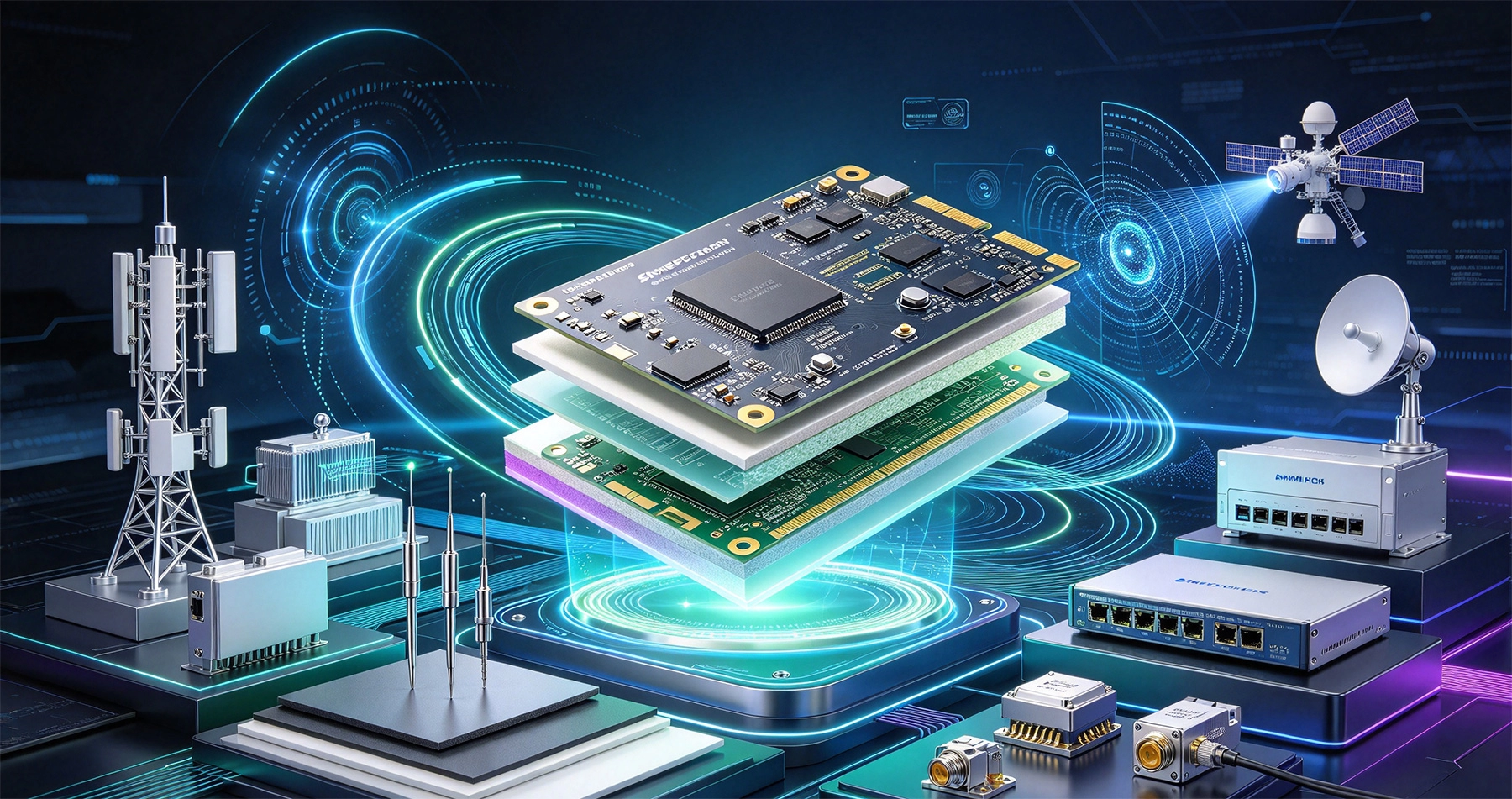
high frequency PCB materials are typically defined as substrates that operate above 5 GHz with low Dielectric Constant (Dk) and low dielectric loss (Df). As signal frequency increases, energy loss in the dielectric and conductor becomes much more significant. A material that works well at 1 or 2 GHz may cause unacceptable attenuation, phase distortion, or impedance variation at 28 GHz, 60 GHz, or higher.
For next-gen communication systems, the key material requirements include:
These requirements are becoming stricter because 5G base stations, mmWave antennas, satellite payloads, and future 6G systems all demand both high bandwidth and high reliability.
Polytetrafluoroethylene (Ptfe) continues to be one of the most important High Frequency Materials for RF and microwave applications. Ptfe-based laminates offer extremely low dielectric loss and very stable electrical performance across wide frequency ranges.
Typical PTFE materials can support applications from 10 GHz to well above 100 GHz, making them suitable for Satellite Communications, radar systems, mmWave front ends, and high-frequency test equipment. Ceramic-filled PTFE variants are also widely used because they improve dimensional stability, thermal conductivity, and manufacturability compared with pure PTFE.
However, PTFE is not easy to process. It has low surface energy, poor adhesion to copper, and requires specialized drilling, desmear, and metallization processes. Plasma treatment or sodium etching is often needed before hole plating. These processing challenges keep costs higher than conventional Fr-4 systems, but for many high frequency designs, the electrical performance advantage is still worth it.
While PTFE offers excellent electrical performance, modified non-PTFE resins are gaining ground. Polyphenylene oxide (PPO/PPE), hydrocarbon resins, benzoxazine, and bismaleimide (BMI) resins are becoming mainstream choices for high speed and high frequency PCBs.
PPO-based laminates, such as those represented by the Megtron family, are widely used in high speed servers, switches, routers, and optical modules. They provide low loss, good thermal reliability, and better process compatibility than many PTFE systems. Hydrocarbon resins are also advancing quickly. Some ultra-low-loss hydrocarbon systems are now approaching PTFE-level performance in certain frequency ranges, especially for M8 and M9 class platforms.
For communication hardware that does not require extreme mmWave performance, these materials often provide a better balance between electrical performance, manufacturing yield, and cost. That balance is one reason they are expanding from data centers into 5G infrastructure, Automotive Radar, and satellite communication modules.
Liquid crystal polymer (LCP) and modified polyimide (PI) materials are attracting more attention for flexible and compact RF designs. LCP offers low dielectric loss, low moisture absorption, and good dimensional stability, which makes it attractive for antenna modules, flexible interconnects, and millimeter-wave packaging.
In next-gen communication devices, space is often limited and mechanical flexibility matters. LCP-based circuits can support high frequency signal routing in thin, lightweight structures. Modified PI materials are also being improved for higher frequency use, although their loss performance generally remains higher than LCP or PTFE at mmWave bands.
These materials are especially relevant for:
The challenge is not only electrical performance. LCP lamination, bonding, and coverlay processes require careful control, and material costs remain relatively high for mass consumer applications.
Another clear trend is the migration toward ultra-low-loss material grades. In high speed PCB design, materials are often classified by loss level, with higher grades representing lower Signal Loss. M6 and M7 materials have been widely adopted for 56 Gbps and 112 Gbps systems, while M8 and M9 grades are increasingly required for 224 Gbps platforms and next-generation Ai Servers.
Although much of this demand comes from AI computing and high speed data centers, it also influences communication hardware. High speed switches, optical modules, backplanes, and baseband units all benefit from lower-loss substrates. As serial data rates increase, the boundary between "high speed digital" and "high frequency RF" becomes less clear.
For communication PCBs, this means material selection can no longer be based only on Dk and Df at a single frequency. Engineers must also consider copper roughness, glass fiber type, resin content, impedance stability, and manufacturing tolerance across the full operating band.
Few communication systems can afford to build every layer from the most expensive high frequency material. Instead, hybrid or mixed-material stack-ups are becoming common. In these designs, high frequency signal layers use Low-loss Materials such as PTFE, hydrocarbon ceramic, or PPO-based laminates, while structural layers use more cost-effective Fr-4 or mid-loss materials.
Hybrid stack-ups help reduce cost without sacrificing RF performance in critical areas. However, they also introduce manufacturing complexity. Different materials have different thermal expansion coefficients, flow characteristics, and lamination temperatures. If the stack-up is not designed carefully, the board may suffer from warpage, delamination, or registration errors.
Best practices for hybrid high frequency boards include:
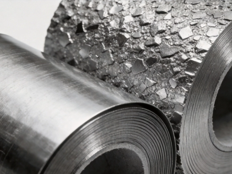
At high frequencies, conductor loss becomes as important as dielectric loss. Surface roughness on copper foil increases the effective current path due to the Skin Effect, which raises Insertion Loss. That is why very low profile (VLP) and hyper very low profile (HVLP) copper foils are increasingly used in high frequency and high speed PCBs.
Glass fiber weave effect is another issue that often surprises designers. Standard woven glass cloth creates local variations in resin and glass content, which can cause periodic impedance fluctuations. For sensitive RF or high speed differential pairs, spread glass, flat glass, or low-Dk glass cloth can improve signal consistency.
In short, material selection is not only about the resin system. Copper foil type, glass style, resin content, and lamination structure all interact to determine real-world performance.
Sustainability is no longer a side topic for Pcb Materials. Regulatory frameworks such as PFAS restrictions in Europe are pushing material suppliers to review fluoropolymer chemistries, halogen-free flame retardants, and long-term compliance risks. At the same time, e-waste reduction and recyclability are becoming more important for consumer electronics and communication infrastructure.
Some emerging research is even exploring bio-based or biodegradable Pcb Materials for lower-frequency wireless applications. While these materials are not yet ready to replace high performance PTFE or PPO systems in mmWave communication, they show where the industry may head for certain consumer and IoT products.
For design teams, the practical takeaway is to check material declarations early. A laminate that meets electrical requirements today may face supply or compliance issues tomorrow, especially in global markets.
Material selection should start with the application, not with a datasheet headline. A good selection process usually follows these steps:
It is also helpful to involve the Pcb Manufacturer during the material selection stage. Simulation models, impedance coupons, and test coupons should reflect the actual laminate, copper foil, and process that will be used in production.
High Frequency Materials focus on stable RF performance at GHz and mmWave frequencies, while high speed materials focus on low loss for fast digital signals. In practice, the two are increasingly overlapping because modern communication systems use both RF and high speed digital interfaces.
Not always. PTFE offers excellent electrical performance, but it is more difficult and expensive to manufacture. For many 5G and high speed communication applications, hydrocarbon ceramic or PPO-based materials provide a better balance of performance, cost, and yield.
FR-4 may still be used for low frequency control circuits, power layers, or non-critical sections. However, for RF paths, mmWave antennas, and high speed backplanes, Low-loss Materials are usually required to meet Signal Integrity targets.
Early 6G research points to ultra-low-loss PTFE, advanced hydrocarbon resins, LCP, modified PI, and possibly new composite substrates. The exact material landscape will depend on frequency bands, system architecture, and manufacturing maturity.
Emerging trends in high frequency pcb materials for next-gen communication are moving in several directions at once. PTFE remains a performance leader for mmWave and satellite applications, while PPO, hydrocarbon, and BMI resins are expanding into high speed communication and infrastructure boards. LCP and modified PI are enabling more flexible and compact RF designs, and ultra-low-loss grades continue to push system performance higher.
At the same time, hybrid stack-ups, low-profile copper foils, low-Dk glass fabrics, and sustainability requirements are making material selection more complex. For engineers and procurement teams, the best strategy is to evaluate electrical performance, manufacturability, supply stability, and regulatory compliance together. high frequency pcb design is no longer just about choosing a low Dk number. It is about building a reliable material system that can survive real production and real operating conditions.
The Impact of Copper Foil Type on High Frequency PCB Materials PerformanceSeptember/16/2026
Rogers vs. FR4: Choosing the Right High Frequency PCB MaterialsJune/12/2026
How Dielectric Constant (Dk) and Loss Factor (Df) Affect High Frequency PCB MaterialsJuly/18/2026
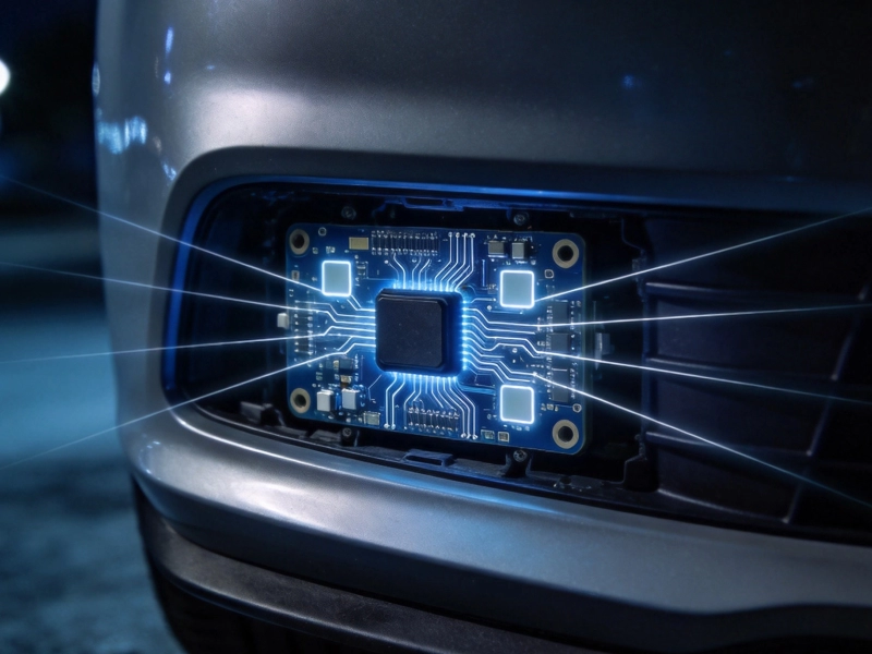
High Frequency PCB Materials for Automotive Radar: Durability and SpeedSeptember/26/2026
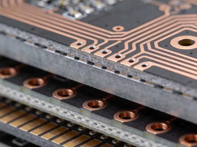
Understanding Thermal Stability in High Frequency PCB MaterialsAugust/10/2026
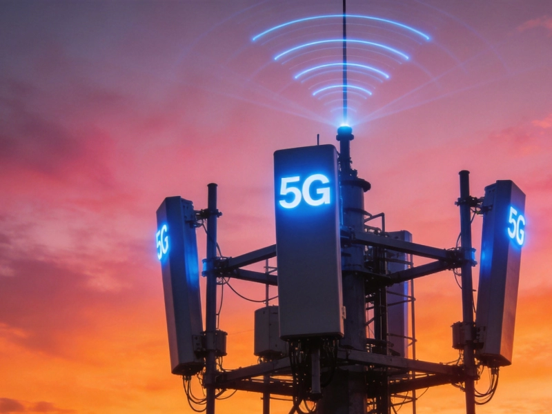
Top 5 High Frequency PCB Materials for 5G Base Station ApplicationsJuly/30/2026
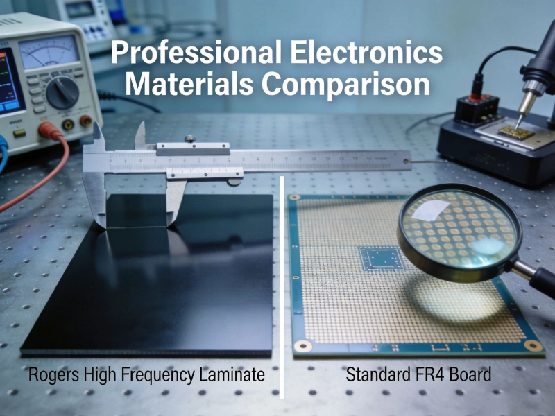
Choosing the Right High Frequency PCB MaterialsMay/29/2026
The Ultimate Guide to High Frequency PCB Materials: PTFE, Ceramic, and HydrocarbonJuly/08/2026