Open Nav

In high frequency PCB design, the dielectric material typically receives most of the attention. Engineers spend considerable effort evaluating loss tangent, Dielectric Constant, and thermal stability of substrate materials. Yet the copper foil—the conductive medium that actually carries signals—is equally critical to high frequency performance. The type of copper foil, its surface treatment, and its grain structure all influence Insertion Loss, impedance consistency, and ultimately the reliability of RF and Microwave Circuits. Overlooking copper foil selection means accepting performance compromises that no amount of dielectric optimization can overcome.
This article examines how different copper foil types affect high frequency PCB performance, explains the underlying physics, and provides guidance for selecting the appropriate foil for your specific application in 5G communications, radar systems, aerospace, and other demanding RF environments.
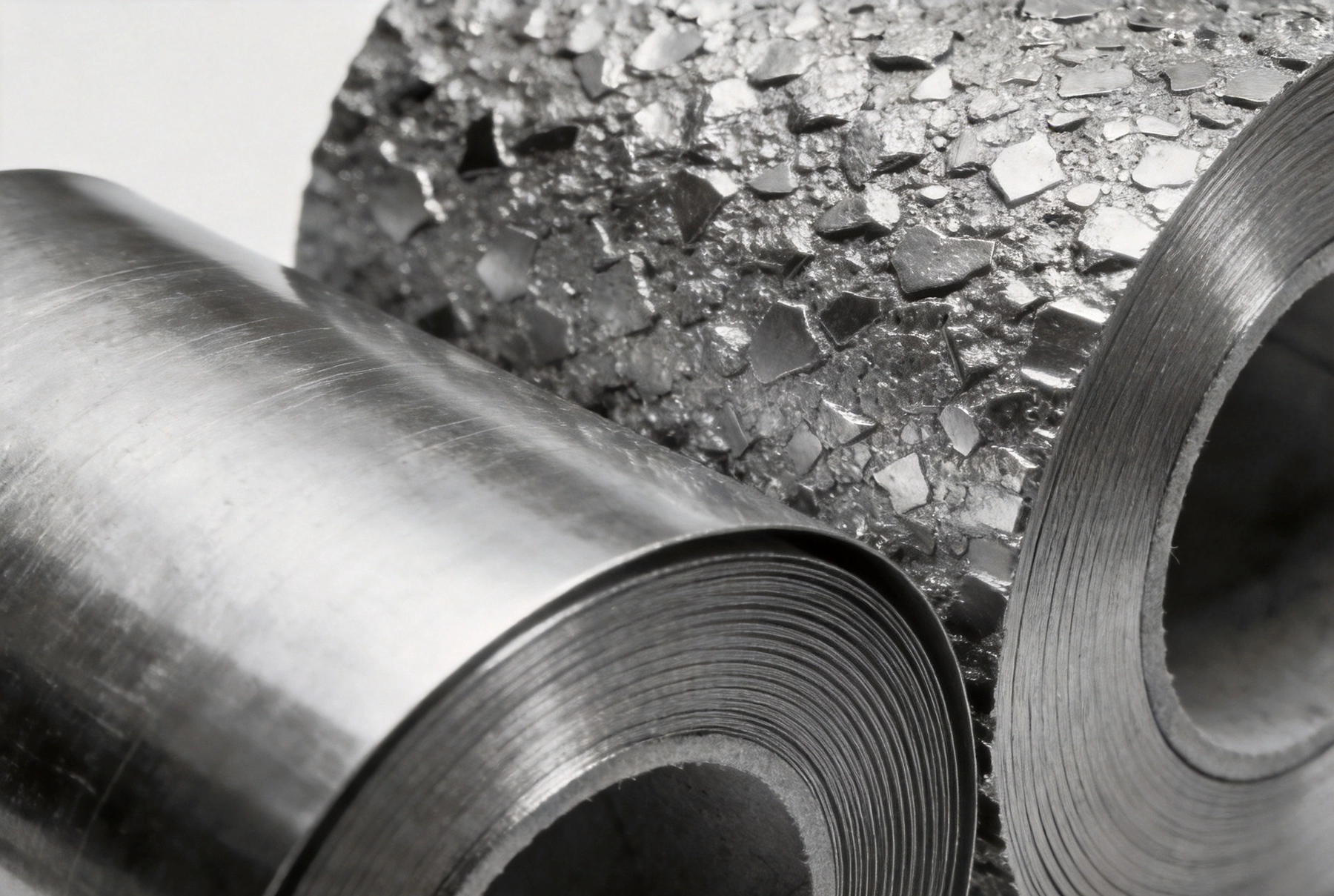
Not all copper foil is manufactured the same way, and the production process directly affects the resulting material properties. Two primary categories dominate high frequency pcb applications: electrodeposited (ED) copper foil and wrought rolled copper foil.
Electrodeposited copper foil is produced by electrolytic plating onto a rotating drum or titanium sheet. Copper ions in solution are reduced at the cathode surface, building up a foil layer of controlled thickness. This process creates a characteristic grain structure with columnar grains oriented perpendicular to the foil surface. The side facing the plating drum—the drum side—is relatively smooth, while the side facing the electrolyte solution—the matte side—exhibits a rougher, nodular surface texture.
ED copper foil is the most widely available and cost-effective option, making it the default choice for most PCB applications. However, its surface roughness and grain structure introduce losses that become significant at high frequencies.
Rolled copper foil is produced by mechanically reducing thick copper stock through successive rolling passes. The process compresses and elongates copper grains in the rolling direction, creating a highly oriented grain structure. This produces a smoother surface finish than ED copper and gives the foil directional properties—electrical and mechanical performance differ along the rolling direction versus across it.
Rolled copper is more expensive than ED foil due to the energy-intensive manufacturing process, but its superior surface smoothness and consistent grain structure make it the preferred choice for the most demanding high frequency applications.
As a compromise between ED and rolled foil, reverse-treated copper foil uses surface treatment processes to reduce the matte side roughness, creating a more uniform surface on both sides. While not as smooth as true rolled copper, RT foil offers improved high frequency performance over standard ED foil at a lower cost premium than rolled copper.
To understand why foil type matters at high frequencies, we must examine the loss mechanisms that affect signal propagation in conductors.
At DC, current distributes uniformly across a conductor's cross-section. As frequency increases, electromagnetic fields induce currents that cancel in the conductor center, forcing current to flow near the surface. This Skin Effect means effective current-carrying cross-section shrinks with increasing frequency, increasing effective resistance.
The skin depth—the depth at which current density falls to 1/e of its surface value—decreases with the square root of frequency. At 1 GHz, skin depth in copper is approximately 2.1 microns. At 10 GHz, it drops to about 0.66 microns. This means signal current flows in only the outermost few microns of the conductor, making surface characteristics critically important.
The rough surface of standard ED copper foil creates a longer effective signal path compared to its geometric dimensions. Current must follow the irregular contours of the foil surface, effectively increasing the resistance beyond what smooth copper would exhibit. This roughness loss becomes increasingly significant as frequency rises and skin depth shrinks toward the scale of surface irregularities.
Surface roughness is typically characterized by root mean square (RMS) values. Standard ED copper foil might exhibit RMS roughness of 2 to 4 microns on the matte side. Low-profile ED foil reduces this to 1 to 2 microns. Very low profile (VLP) foil achieves 0.3 to 0.7 microns. Rolled copper reaches 0.1 to 0.4 microns—approximately an order of magnitude smoother than standard ED foil.
The impact on Insertion Loss compounds across the board's operating frequency range. At frequencies below 5 GHz, roughness differences might contribute 5% to 10% additional loss for rough versus smooth foil. At 30 GHz and above, the same comparison might show 30% or greater loss differential. For 5G millimeter-wave applications operating at 28 GHz, 39 GHz, or 77 GHz Automotive Radar frequencies, foil type choice can be the difference between meeting and missing loss budgets.
In high density layouts with traces spaced closely together, the magnetic fields of adjacent conductors influence current distribution, creating additional losses beyond Skin Effect alone. The proximity effect is particularly significant in multilayer boards with traces running parallel in adjacent layers. Careful layer assignment and spacing help mitigate proximity effect, but the underlying loss mechanism remains tied to the conductor's surface characteristics.
Raw copper foil requires surface treatments to ensure reliable adhesion to the substrate and to protect against oxidation. These treatments, while necessary for manufacturing, affect high frequency performance in ways that designers should understand.
The foil's bonding side receives treatments that create a mechanical interlocking surface for the prepreg resin. Standard treatments create the nodular profile visible under magnification. For high frequency applications, low-profile treatments minimize surface irregularity while maintaining adequate bonding strength.
Some manufacturers offer specifically engineered treatments that minimize surface profile while still achieving acceptable peel strength values. These treatments sacrifice some adhesion performance for improved electrical characteristics, a worthwhile trade-off for RF boards where Signal Integrity takes priority.
Coatings applied to prevent oxidation during storage and processing can affect solderability and high frequency performance. Chromium-based and benzotriazole-based treatments are common. These coatings are typically thin enough that they do not significantly affect RF performance, but very rough anti-tarnish layers could contribute to losses. Manufacturer data sheets should specify coating thickness and composition for evaluation.
Ultra-thin copper foils (below 18 microns) are difficult to handle during Pcb Manufacturing. To address this, manufacturers apply the ultra-thin foil to a carrier foil—typically standard copper or aluminum—that provides mechanical support during processing. After lamination, the carrier is separated, leaving the ultra-thin foil bonded to the substrate.
Carrier foil systems enable the use of ultra-thin conductors that would otherwise be impossible to process. At high frequencies, the thin conductor ensures the entire cross-section carries current, potentially improving performance for specific trace geometries. However, the interface between ultra-thin foil and substrate can introduce additional discontinuities that must be considered during design.
High frequency circuits require precise Impedance Control to prevent signal reflections. Copper foil characteristics affect impedance in ways that must be accounted for during design and manufacturing.
For a given target impedance, trace width calculations assume a specific conductor profile. Rough foil with irregular edges creates effective trace widths different from the nominal drawn dimensions. The current crowding at surface irregularities effectively narrows the current-carrying width, changing the trace's Characteristic Impedance.
This effect becomes more pronounced as trace widths shrink. At 50-micron trace widths common in high density designs, a 2-micron roughness represents 4% of the trace width. The same roughness on a 200-micron power bus trace represents only 1% of width. Designers specifying impedance for fine traces must account for this scaling effect.
Rolled copper's consistent surface profile produces more repeatable impedance across a board compared to ED foil, where surface roughness varies more between lots and across the sheet. For applications requiring tight impedance tolerance, rolled copper's consistency advantage translates directly to higher yield and more predictable performance.
When impedance tolerance of ±5% or tighter is required, the foil type and its uniformity should be specified as part of the manufacturing requirements. Many high frequency pcb manufacturers maintain statistical process data showing impedance variation attributable to foil type and can advise on achievable tolerances for specific constructions.
Different application frequency ranges face different loss budgets and performance requirements. Understanding these requirements helps guide foil type selection.
The sub-6 GHz spectrum used in early 5G deployments (600 MHz to 6 GHz) remains the most commercially significant high frequency range. At these frequencies, standard low-profile ED copper foil typically provides acceptable performance for many applications. Insertion loss budgets are usually achievable with careful design even using standard ED foil.
However, base station equipment and active antenna systems with multiple RF chains benefit from lower-loss rolled copper. The cumulative loss reduction across dozens of RF channels in a massive MIMO antenna adds up to meaningful system-level power savings and reduced heat generation.
High frequency 5G bands at 24 GHz, 28 GHz, 39 GHz, and the emerging 47 GHz and 71 GHz ranges place much more stringent demands on copper foil performance. Skin depth at these frequencies approaches the scale of standard foil roughness, making rolled copper or very low profile ED foil essentially mandatory for acceptable performance.
Automotive Radar at 77 GHz and 79 GHz pushes this requirement even further. The loss budgets for these applications are extremely tight, and foil roughness directly affects the achievable range and resolution of the radar system. Rolled copper foil is the standard choice for automotive radar modules for good reason.
Weather radar, air traffic control radar, and aerospace communication systems operating across wide frequency ranges require consistent performance that only high-quality copper foil provides. These systems often have multi-decade service lives and must maintain performance despite environmental exposure and aging.
The initial investment in premium foil types pays dividends over the system lifetime through reduced maintenance, fewer replacements, and more consistent performance tracking against specifications.
Satellite payloads face the additional challenge of radiation exposure that can affect material properties over time. Foil type selection for space applications considers not just electrical performance but also radiation hardness and long-term stability. Rolled copper with its consistent grain structure may offer advantages in radiation environments, though specific qualification testing is required for space applications.
Selecting the appropriate copper foil requires balancing electrical performance, cost, and manufacturing considerations.
Begin by establishing the frequency range and loss budget for your application. For applications below 10 GHz with moderate loss budgets, low-profile ED copper foil typically suffices. For applications above 10 GHz or with stringent loss requirements, consider very low profile ED or rolled copper foil. For millimeter-wave applications above 30 GHz, rolled copper is the safest choice.
Next, consider impedance tolerance requirements. Tighter tolerances favor smoother foil types due to their more consistent impedance performance. If your design requires ±5% impedance tolerance at frequencies above 10 GHz, the additional cost of rolled copper is likely justified.
Finally, evaluate manufacturing compatibility. Rolled copper foil requires different handling and processing parameters than ED foil. Not all manufacturers have experience with rolled copper. Verify your assembly partner's capabilities and process parameters for the foil type you specify.
When specifying copper foil for high frequency applications, clearly communicate the following requirements:
Request surface profile data from your manufacturer as part of the qualification process. This data enables correlation with electrical performance measurements and builds confidence in the material specification.
Verifying that copper foil performs as expected requires appropriate testing that goes beyond standard PCB acceptance tests.
Atomic force microscopy (AFM) or optical interferometry provide quantitative surface roughness measurements. Request these measurements from your foil supplier or use them as part of incoming inspection for critical applications. The data confirms that received material meets roughness specifications.
Fabricate test coupons with Controlled Impedance traces of known geometry on the target laminate and foil combination. Measure insertion loss using vector network analysis to establish baseline performance. Compare measured loss against theoretical predictions accounting for skin effect and surface roughness models.
This testing validates that the foil specification produces the expected electrical performance and identifies any unexpected losses that might indicate process or material issues.
For boards with tight impedance requirements, time-domain reflectometry (Tdr) mapping across the board surface reveals impedance uniformity. High-impedance mapping uniformity correlates with consistent foil characteristics and good process control. Poor uniformity indicates sources of variation—including foil roughness variation—that should be addressed before production.
The impact varies significantly with frequency. At 1 GHz, the difference between standard ED foil and rolled copper might add 0.1 to 0.2 dB per inch of trace. At 28 GHz—the 5G mmWave band—this difference could reach 0.5 to 1.0 dB per inch. For a 10-inch RF path, the cumulative difference could exceed 10 dB, potentially requiring additional amplifier stages or compromising system sensitivity. In mmWave applications, foil type can represent the difference between a viable and impractical design.
While technically possible with extreme care, using standard materials for 77 GHz is strongly discouraged. At 77 GHz, skin depth in copper is approximately 0.24 microns—smaller than the surface roughness of standard ED foil. The effective conductor loss becomes dominated by surface texture. Successful 77 GHz designs universally use rolled copper foil and ultra-low-loss Dielectric Materials specifically engineered for mmWave frequencies.
Copper foil type has minimal direct impact on thermal conductivity perpendicular to the board plane, which is dominated by the dielectric material. However, for high current applications, the foil's current-carrying capacity and thermal resistance of traces carrying high-frequency AC currents are affected by surface characteristics. In mixed-signal boards combining high-frequency and high-current sections, consider foil type for both concerns.
Differential pairs are particularly sensitive to foil uniformity because skin effect and roughness affect both conductors of the pair identically, but slight differences in local roughness can create imbalances. For high-speed differential interfaces like 56 Gbps SerDes or emerging 112 Gbps links, rolled copper foil provides the most consistent coupling between pair members. Even small imbalances compound at these data rates, affecting jitter and eye opening.
Rolled copper foil typically costs 2 to 4 times more than standard ED foil on a per-area basis. For a typical RF board representing $10 to $20 in foil cost, the premium might be $20 to $60 per board—modest relative to total board cost but significant in high-volume production. Evaluate this premium against the performance benefits for your specific application. At millimeter-wave frequencies, the electrical performance advantage typically justifies the cost. At sub-10 GHz frequencies with relaxed loss budgets, the premium may not be warranted.
Copper foil type is a critical yet often overlooked factor in High Frequency Pcb design. The surface roughness, grain structure, and treatment of the foil directly influence insertion loss, impedance consistency, and ultimately the electrical performance of RF and Microwave Circuits. As operating frequencies increase toward 5G mmWave bands and automotive radar frequencies, these effects become more pronounced, making foil selection increasingly important.
Standard electrodeposited copper foil with its rough surface texture suffices for many sub-10 GHz applications but introduces losses that become unacceptable at higher frequencies. Very low profile ED foil and reverse-treated foil offer improved performance at moderate cost premiums. Rolled copper foil, with its ultra-smooth surface and consistent grain structure, provides the best high frequency performance and impedance consistency but at a higher cost.
For 5G infrastructure, automotive radar, and other demanding RF applications, the additional cost of premium foil types is justified by improved electrical performance, better yield, and more consistent manufacturing. Specify foil requirements clearly, validate performance through appropriate testing, and work with manufacturers experienced in High Frequency Materials to ensure the delivered boards meet the demanding requirements of modern RF systems.
Understanding the interplay between dielectric material, copper foil, and design geometry enables creating high frequency circuits that achieve their performance targets while remaining manufacturable and cost-effective. The investment in proper material selection—dielectric and conductor—pays dividends across the product lifecycle in improved performance, higher yield, and reliable field operation.
Ready to explore copper foil options for your High Frequency Pcb design? Connect with an engineering team experienced in RF and mmWave applications to evaluate the optimal foil type for your specific performance requirements.
Rogers vs. FR4: Choosing the Right High Frequency PCB MaterialsJune/12/2026
Cost vs. Performance: Selecting Budget-Friendly High Frequency PCB MaterialsSeptember/04/2026
Understanding Thermal Stability in High Frequency PCB MaterialsAugust/10/2026

Top 5 High Frequency PCB Materials for 5G Base Station ApplicationsJuly/30/2026

How Dielectric Constant (Dk) and Loss Factor (Df) Affect High Frequency PCB MaterialsJuly/18/2026
The Ultimate Guide to High Frequency PCB Materials: PTFE, Ceramic, and HydrocarbonJuly/08/2026
Choosing the Right High Frequency PCB MaterialsMay/29/2026
Handling Sensitive ComponentsMay/29/2026