Open Nav

High frequency printed circuit boards are used in applications where Signal Integrity, Controlled Impedance, and low loss are critical. These include radar systems, Satellite Communications, 5G infrastructure, millimeter-wave modules, automotive sensors, and high-speed digital platforms. In these designs, the PCB material is not just a mechanical support. It is an active part of the electrical system.
Unlike standard Fr-4 boards, High Frequency Materials are more sensitive to variations in Dielectric Constant, loss tangent, thickness, copper roughness, and manufacturing consistency. Small deviations can affect Insertion Loss, phase stability, Impedance Control, and overall system performance. Therefore, testing and verifying high frequency PCB materials is essential before and after production.
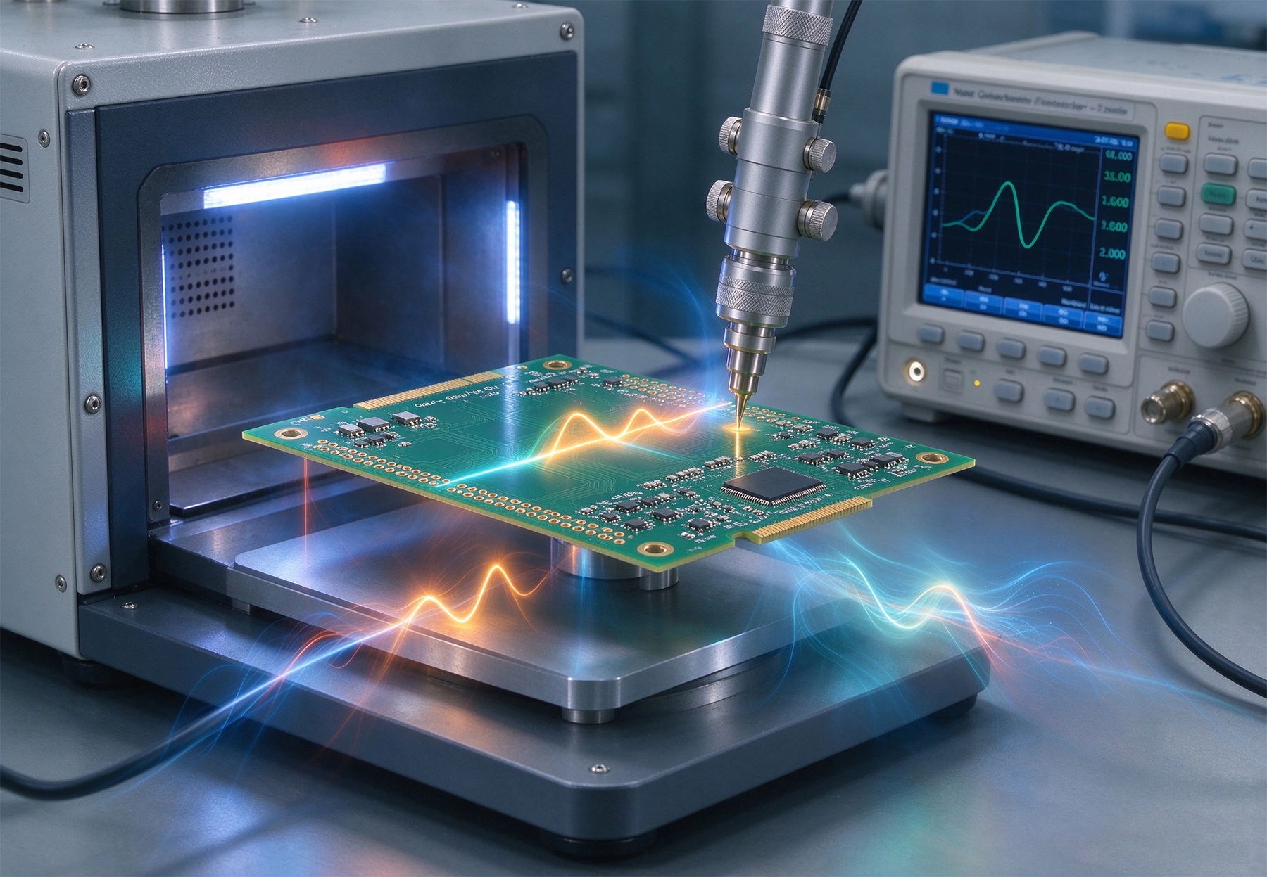
At low frequencies, many PCB parameters have limited impact on circuit behavior. As frequency increases, however, the substrate begins to influence signal propagation more strongly. Dielectric Constant determines signal velocity and impedance. Loss tangent affects energy dissipation. Thickness variation changes impedance. Copper Surface Roughness increases conductor loss at higher frequencies.
High Frequency Materials such as Ptfe-based laminates, ceramic-filled hydrocarbons, and engineered thermoset systems are often chosen for their stable electrical properties. But these materials can be more difficult to process than conventional Fr-4. They may require special drilling, plating, lamination, and surface treatment processes. Without proper verification, a material that looks suitable on paper may underperform in real applications.
The dielectric constant, often expressed as Dk, describes how much the material slows down an electromagnetic wave compared with free space. It directly affects impedance calculation, phase length, and resonant frequency. For high frequency designs, Dk stability across frequency and temperature is often more important than the nominal value alone.
Verification should confirm that the material meets the specified Dk range and that the value is consistent across the laminate sheet and production lot.
Loss tangent, or Dissipation Factor, indicates how much signal energy is absorbed by the dielectric material. A lower loss tangent generally means lower Insertion Loss, which is critical for antennas, filters, amplifiers, and high-speed Transmission Lines.
Because loss increases with frequency, even small differences in loss tangent can become significant at millimeter-wave frequencies. Testing should verify that the material meets the required loss performance for the intended operating band.
Laminate thickness affects impedance, capacitance, and mechanical fit. High frequency circuits often require tight thickness control because small changes can shift impedance and degrade return loss. Total thickness includes core, prepreg, copper foil, and any surface finish.
Verification should include measurement of finished board thickness and dielectric thickness at multiple locations to confirm uniformity.
Copper foil roughness influences conductor loss at high frequencies. As frequency increases, current flows closer to the conductor surface due to the Skin Effect. Rougher copper increases the effective current path and raises insertion loss.
For high frequency and millimeter-wave applications, low-profile or very-low-profile copper foil is often preferred. Verification may include reviewing foil specifications, cross-section analysis, or electrical loss comparison.
High frequency boards may experience temperature changes during operation, testing, or assembly. Materials must maintain stable electrical properties across the expected temperature range. Important indicators include coefficient of thermal expansion, decomposition temperature, and moisture absorption.
Excessive moisture absorption can change dielectric properties and reduce reliability. Thermal instability can cause dimensional changes, via stress, or delamination during reflow soldering.
Quality verification begins before fabrication. When high frequency laminates arrive from material suppliers or PCB manufacturers, incoming inspection helps confirm that the correct material has been supplied and that it has been stored properly.
Typical incoming checks include:
For critical programs, customers may request additional test reports such as Dk/Df verification, thickness measurement, or glass style confirmation.
Ring resonator structures are commonly used to extract dielectric constant and loss tangent from fabricated test coupons. These structures resonate at specific frequencies, allowing engineers to calculate material properties based on measured response.
Coupon testing is useful because it evaluates the material after lamination and processing, not just in raw form. This provides a more realistic view of how the material will perform in actual boards.
Microstrip or stripline test structures can be used to measure insertion loss over frequency. By comparing measured loss with simulated models, engineers can assess whether the material and process meet expectations.
This method is practical because it reflects real signal paths. It helps identify issues caused by copper roughness, dielectric variation, surface finish, or manufacturing tolerance.
Time domain reflectometry, or Tdr, is widely used to verify Controlled Impedance. A fast edge signal is sent through a Transmission Line, and reflections are analyzed to determine impedance along the path.
Tdr Testing is especially important for high speed digital and RF boards where impedance mismatches can cause signal distortion, jitter, or return loss problems.
Vector network analyzers provide detailed S-parameter measurements, including insertion loss, return loss, phase response, and isolation. These measurements are essential for validating high frequency performance.
Vna Testing can be performed on test coupons, evaluation boards, or finished assemblies. It allows engineers to compare actual performance with simulation and identify deviations caused by material or process variation.
Cross-sectioning reveals internal board structure, including dielectric thickness, copper thickness, via quality, and layer registration. For high frequency boards, consistent dielectric thickness is critical for Impedance Control.
Cross-section analysis can also detect voids, delamination, insufficient plating, or resin starvation that may not be visible from the surface.
High frequency materials sometimes require special via preparation due to their chemical or mechanical properties. Microsection inspection helps verify via wall quality, barrel plating thickness, and annular ring integrity.
For Ptfe-based materials, via reliability depends heavily on proper pretreatment and plating adhesion. Poor via quality can lead to intermittent failures even if electrical testing initially passes.
Thermal cycling tests evaluate how materials and structures respond to repeated temperature changes. This is important for boards that will operate in automotive, aerospace, outdoor communication, or industrial environments.
After thermal cycling, boards can be re-inspected for delamination, via cracks, impedance shift, or increased insertion loss. These tests help confirm long-term reliability.
Some high frequency materials absorb more moisture than others. Moisture can change dielectric properties and reduce insulation performance. For outdoor or high-reliability applications, moisture absorption should be reviewed during material selection and qualification.
Verification may include comparing material specifications, reviewing test reports, or performing controlled humidity exposure followed by electrical measurement.
Surface finish affects both solderability and high frequency performance. Common finishes include ENIG, ENEPIG, immersion silver, immersion tin, OSP, and gold plating. Each has different effects on insertion loss, wire bonding, and shelf life.
For millimeter-wave circuits, thicker or rougher surface finishes may increase conductor loss. Verification should include surface finish thickness measurement and electrical comparison where necessary.
Impedance control is one of the most important quality indicators for high frequency and high speed boards. Manufacturers typically perform impedance testing using Tdr on dedicated test coupons included in the panel.
Customers should verify that impedance targets, tolerance ranges, test structures, and measurement methods are agreed upon before production. Post-production impedance reports should be reviewed against design requirements.
High frequency boards often include fine features such as narrow Transmission Lines, small gaps, and precise antenna structures. Dimensional stability during fabrication affects pattern accuracy and electrical performance.
Verification may include optical inspection, dimensional measurement, and registration checks between layers. Excessive dimensional variation can cause impedance errors and assembly misalignment.
One common mistake is relying only on nominal Dk and Df values from data sheets without considering frequency dependence, glass style, or resin content. Another is ignoring copper roughness, which can cause higher loss than expected at millimeter-wave frequencies.
Some teams also overlook process compatibility. A material may have excellent electrical properties but require special handling during drilling, plating, or lamination. If the PCB supplier lacks experience with that material, yield and reliability may suffer.
Finally, testing only bare boards without evaluating assembled performance can miss issues introduced by solder mask, surface finish, connectors, or assembly processes. Whenever possible, verification should include both material-level and system-level checks.
Testing and verifying high frequency PCB materials is a multi-step process that combines material review, incoming inspection, electrical measurement, physical analysis, and process validation. The goal is not only to confirm that the material meets its specification, but also to ensure that it performs reliably after fabrication and assembly.
For high frequency and high speed applications, material quality directly affects Signal Integrity, loss, impedance control, and long-term reliability. By establishing a clear verification workflow and working with experienced PCB suppliers, engineering teams can reduce risk, avoid costly redesigns, and achieve more predictable performance in demanding RF and microwave designs.
Dielectric constant and loss tangent are both critical. Dk affects impedance and phase, while loss tangent affects insertion loss. The relative importance depends on the application, frequency range, and circuit topology.
Yes. Test coupons, resonator structures, transmission lines, and TDR patterns can be fabricated alongside production boards to verify material and process performance after lamination and plating.
At high frequencies, current flows near the conductor surface. Rougher copper increases the effective path length and raises conductor loss, which can degrade insertion loss and signal quality.
Standard FR-4 can be used at lower RF frequencies, but its loss and Dk stability are usually insufficient for demanding microwave or millimeter-wave designs. High frequency laminates are preferred when low loss and stable electrical properties are required.
Exploring High Frequency PCB Applications in High-Speed Data CentersSeptember/30/2026
High Frequency PCB Capabilities: Handling Thick Copper and High Power RFSeptember/15/2026
Key High Frequency PCB Knowledge for Successful RF Circuit DesignSeptember/07/2026
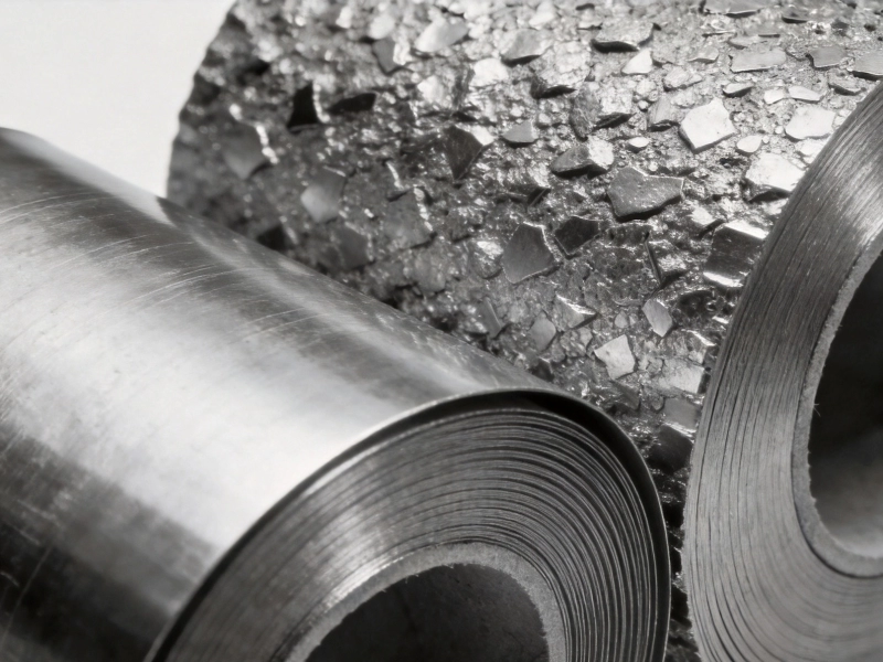
The Impact of Copper Foil Type on High Frequency PCB Materials PerformanceSeptember/16/2026
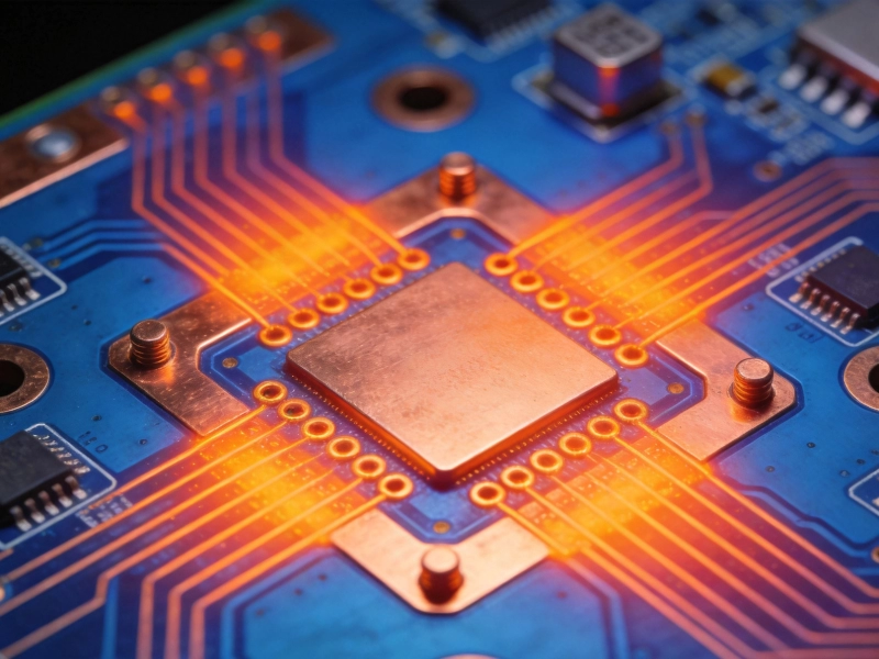
The Importance of Thermal Management in High Frequency PCB AssemblyJuly/27/2026
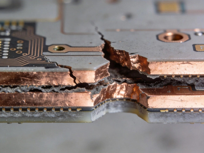
Overcoming Delamination Challenges in Multilayer High Frequency PCB FabricationJuly/28/2026

Our Latest High Frequency PCB Capabilities for 6G ResearchMay/29/2026

High Frequency PCB Knowledge: The Difference Between High-Speed and High-FrequencySeptember/17/2026