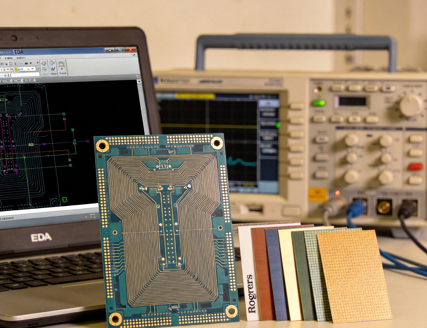
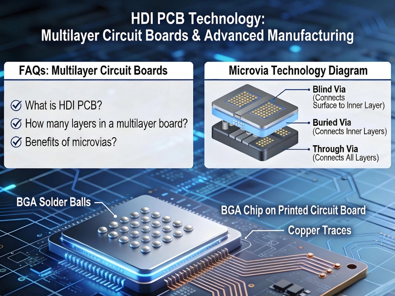
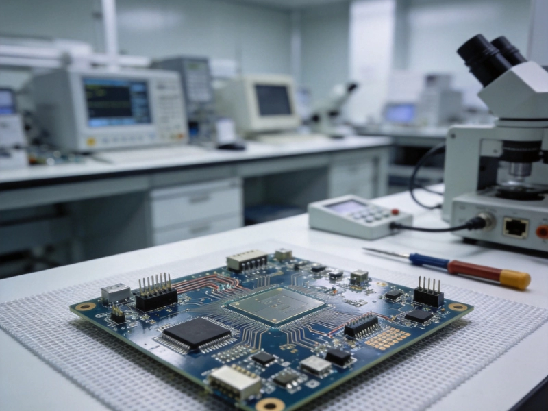
You have spent weeks simulating your 77 GHz radar front-end, tuning the matching networks, and optimizing the antenna-in-package layout. The schematic is clean, the simulation results are promising, and you are ready to build. Now comes the moment where theory meets manufacturing: ordering your high-frequency Pcb Prototype. Get this step right, and you will have a board that validates your design. Get it wrong, and you will spend weeks debugging a prototype that failed not because of your circuit, but because of a stack-up error, a material mismatch, or an impedance tolerance that the fabricator could not hold.
This guide walks through every step of the process—from final design checks through quoting, ordering, and receiving a high-frequency Pcb Prototype that actually works.

Step 1: Finalize Your Design Files
Before you send anything to a fabricator, verify that your design database is complete and consistent. The most common causes of prototype delays and errors are not technical—they are missing or inconsistent data.
Required Files
- Gerber Files (RS-274X) or ODB++ for every copper layer, solder mask, silkscreen, and paste mask. Verify that the aperture list is embedded and the format (integer/decimal places) is consistent across all files.
- Drill file (Excellon format) with both plated and non-plated holes. Confirm that the drill units (inch or mm) match the Gerber units. Mixed units are the single most common file-format error.
- Netlist (IPC-D-356A) for electrical test. Without a netlist, the fabricator can only test for shorts and opens based on Gerber data—which misses split-plane and naming errors.
- Stack-up definition. A written document specifying layer order, material type and thickness for each dielectric, copper weight for each layer, and impedance requirements. This is not optional for high-frequency boards—Gerber Files alone do not define the stack-up.
- Impedance table. A table listing every controlled-impedance trace type, target impedance, tolerance, and the layers on which it appears. Example: "L1 microstrip, 50 Ω ±5 %, trace width 7.2 mil; L3-L4 stripline, 100 Ω diff ±7 %, trace width 4.5 mil, space 5.0 mil."
Pre-Submission Checks
- Run your CAD tool's DRC (design rule check) one final time. Fix every violation—do not waive them for prototype runs, because waived violations are the ones that cause manufacturing failures.
- Verify that every controlled-impedance trace has a continuous reference plane on the adjacent layer. A microstrip trace crossing a plane split is an impedance discontinuity that simulation may not catch.
- Confirm that component land patterns match the manufacturer's recommended footprint. A 0.2 mm pad-size error on a 0.4 mm pitch BGA can cause opens or shorts after reflow.
- Check that via-to-trace and trace-to-trace clearances meet the fabricator's minimum capability. High-frequency designs often push these limits; verify that you are within the fab's stated limits for the copper weight and line/space you have specified.
Step 2: Select the Right Material
Material selection is the most consequential decision in a high-frequency PCB prototype—and the one most often delegated to the fabricator's default. For frequencies above 2 GHz, standard Fr-4 is almost always the wrong choice. The key parameters are:
Dielectric Constant (Dk) and Its Stability
- Dk value determines trace width for a given impedance and dielectric thickness. Lower Dk enables wider traces (easier to manufacture) or thinner dielectrics (thinner boards).
- Dk tolerance matters more than the nominal value. A material with Dk 3.0 ±0.04 is far more useful for Controlled Impedance than one with Dk 3.0 ±0.2, even though the nominal is the same.
- Dk vs. frequency. Dk decreases with frequency for most laminates. Always use the Dk value at your operating frequency, not the 1 MHz or 10 GHz datasheet value. Request Dk data at your specific frequency from the laminate manufacturer.
Dissipation Factor (Df) — Dielectric Loss
- Df directly determines Insertion Loss per unit length. At 10 GHz, Insertion Loss in dB/in. is approximately proportional to (Df × √Dk × frequency). A material with Df 0.002 has roughly 10× lower loss than Fr-4 (Df ≈ 0.02) at the same frequency.
- For 77 GHz Automotive Radar, target Df ≤ 0.002. For sub-6 GHz RF, Df ≤ 0.005 is usually adequate. For high-speed digital (SerDes at 10+ Gbps), Df ≤ 0.005 with stable Dk is the key criterion.
Common High-Frequency Material Choices
- Rogers RO3003G2: Dk 3.0, Df 0.0013 at 77 GHz. The gold standard for mmWave radar and antenna modules.
- Rogers Ro4350b: Dk 3.48, Df 0.0037. Process-compatible with FR-4 (same lamination temperatures), making it a cost-effective choice for 2–30 GHz applications.
- Rogers RT/duroid 5880: Dk 2.2, Df 0.0009. Ultra-low loss for satellite and defense applications. Mechanically soft—requires careful handling.
- Panasonic Megtron 6: Dk 3.4, Df 0.002. Excellent for high-speed digital backplanes and mixed RF/digital boards.
- Isola I-tera MT40: Dk 3.38, Df 0.0035. FR-4 process-compatible, good for 5–15 GHz and cost-sensitive applications.
Hybrid Stack-Ups
Most high-frequency prototypes use a hybrid stack-up: high-frequency laminate on the outer layers (where RF traces and antennas live) and standard or low-loss FR-4 on inner layers (for power, ground, and digital routing). This reduces material cost while preserving RF performance where it matters. Ensure your stack-up document clearly specifies which material goes on which layer—ambiguous material calls lead to wrong builds.
Step 3: Define the Stack-Up and Impedance Requirements
The stack-up is the cross-sectional recipe for your board. For a high-frequency prototype, it must be specified in writing and agreed with the fabricator before manufacturing begins.
Stack-Up Document Contents
- Layer-by-layer listing: layer number, function (signal, ground, power), copper weight, material type and thickness.
- Total finished board thickness and tolerance.
- Prepreg type and resin content between each layer pair (this determines dielectric thickness and Dk).
- Controlled-impedance requirements: trace type (microstrip, stripline, coplanar waveguide), target impedance, tolerance, reference layer(s), and calculated trace width.
- Solder mask inclusion/exclusion for RF layers (solder mask is lossy at mmWave frequencies; many 77 GHz boards specify solder mask openings over RF traces).
Working with the Fabricator on Stack-Up
Do not simply impose a stack-up on the fabricator—collaborate. The fabricator knows which prepreg styles and resin contents they stock, which material combinations have proven lamination results, and what dielectric thicknesses they can reliably achieve. A collaborative stack-up review typically follows this sequence:
- You provide your target stack-up and impedance requirements.
- The fabricator's CAM engineer reviews it, verifies impedance calculations with their own solver, and proposes adjustments (e.g., "We recommend 1080 spread-glass prepreg instead of 106 for better thickness control," or "Your 3.5 mil dielectric target requires a specific resin content; we recommend 3.7 mil with 1080 prepreg at 62 % resin for better repeatability").
- You evaluate the proposed adjustments against your simulation results and approve or negotiate.
- The agreed stack-up is documented and signed off by both parties before the order is released.
This collaboration is especially critical for first prototypes, where there is no production history to fall back on. A fabricator who just builds to your drawing without review is one who will build to your errors, too.
Step 4: Conduct a DFM Review
Design for Manufacturing (Dfm) review is a structured check of your design against the fabricator's process capabilities. For high-frequency boards, Dfm goes beyond the standard checks (minimum trace/space, minimum drill, annular ring) to include RF-specific items:
- Material availability. Does the fabricator stock the specified laminate and prepreg, or must they order it? Special-order materials add 2–4 weeks to prototype lead time.
- Lamination compatibility. Can the specified materials be laminated together? PTFE-based laminates (RO3003, RT/duroid) require lower lamination temperatures and different press cycles than FR-4. Mixed PTFE/FR-4 stack-ups need careful cycle design to avoid delamination.
- Etch capability at specified line widths. Can the fab hold the trace widths needed for your impedance targets with the specified copper weight? If your design calls for 3 mil traces on 1 oz copper, the fab must confirm they can achieve this—and at what tolerance.
- Impedance coupon design. Will the fab's standard coupon layout support your impedance types (single-ended 50 Ω, differential 100 Ω, coplanar waveguide), or does the coupon need custom design?
- Solder mask over RF traces. If you need solder mask openings over RF areas, verify that the fab can produce clean, precise openings without bleeding onto adjacent traces.
- Surface finish compatibility. ENIG (electroless nickel / immersion gold) is standard for most prototypes but adds nickel under the gold—a lossy magnetic layer at mmWave frequencies. For 77 GHz traces, consider ENEEP (electroless nickel / electroless palladium / immersion gold) or direct immersion gold without nickel. Confirm the fab's capability for your chosen finish.
Request the DFM review in writing and resolve all findings before releasing the order. A DFM issue found after the boards are built is a very expensive finding.
Step 5: Obtain a Quote and Confirm Specifications
When requesting a quote for a high-frequency prototype, provide more information than you think you need. A thorough quote package prevents surprises:
Quote Package Contents
- Quantity (typical prototype: 5–20 boards).
- Board dimensions and array/panel configuration (if you want the boards delivered in an array for assembly).
- Layer count and stack-up document.
- Material callout for each layer (laminate type, prepreg style, copper weight).
- Minimum finished trace width and spacing.
- Minimum drill size and number of holes.
- Controlled-impedance requirements (impedance table).
- Surface finish (ENIG, HASL, immersion silver, ENEEP, hard gold on fingers).
- Solder mask color and specific openings/clearances.
- Electrical test requirement (netlist-based testing, with impedance testing on coupon).
- Lead time (typical prototype: 5–10 business days for standard materials; 10–15 days for specialty laminates; 15–20 days for PTFE-based materials if not in stock).
Quote Evaluation
Compare quotes on more than price:
- Does the quote include impedance testing? Some fabs quote impedance testing as a line item; others include it. Make sure you are comparing apples to apples.
- Is the material specified or generic? A quote that says "low-loss material" without specifying the laminate manufacturer and grade is a red flag. You may receive a different material than you simulated.
- Lead time realism. A 5-day lead time on a Rogers RO3003G2 board is suspicious unless the fab has the material in stock. Verify material availability before committing.
- First-article inclusion. Does the quote include first-article inspection (cross-section, impedance test report, dimensional measurement)? For a prototype, first-article data is essential—you need to verify that the built board matches the simulated stack-up.
Step 6: Place the Order and Provide Complete Data
Once you have selected a fabricator and confirmed the quote, place the order with these critical elements:
- Purchase order referencing the agreed quote, stack-up document, and impedance specification.
- Design files (Gerber/ODB++, drill, netlist) uploaded to the fab's portal or sent via secure transfer. Verify file integrity after upload—corrupted Gerber files are a real risk.
- Stack-up approval document signed by both parties. This is your insurance: if the built board does not match the agreed stack-up, you have grounds for remake.
- Special instructions in writing: solder mask openings, non-standard surface finish, impedance coupon requirements, first-article requirements.
After the order is placed, the fabricator's CAM department will process your files. They may generate CAM questions—clarifications about drill sizes, layer mappings, or unclear specifications. Respond promptly; CAM questions left unanswered delay the build.
Step 7: Review the CAM Confirmation
Before the fabricator releases the order to production, they will send a CAM confirmation (sometimes called a "production data review" or "pre-production check"). This document shows how the CAM system interpreted your data:
- Layer mapping: confirm that each Gerber file is assigned to the correct physical layer.
- Drill mapping: confirm plated vs. non-plated hole assignment.
- Panel layout: confirm the array configuration and number of boards per panel.
- Etch compensation: verify that the CAM system has applied etch compensation appropriate to your copper weight and line widths.
- Impedance coupon: review the coupon layout and confirm that it includes all your impedance types.
Do not skip this step. CAM misinterpretations—layer swaps, wrong drill types, missing etch compensation—are responsible for a significant fraction of prototype failures.
Step 8: Manufacturing and In-Process Checks
For a high-frequency prototype, the key in-process checkpoints are:
After Inner-Layer Imaging and Etch
- AOI (automated optical inspection) on inner layers to catch shorts, opens, and linewidth errors before lamination. Inner-layer defects are not repairable after lamination.
- First-panel trace-width measurement on inner signal layers, especially for controlled-impedance stripline traces.
After Lamination
- Post-lamination thickness measurement. Compare the measured total thickness and individual layer thicknesses (from cross-section of a test coupon) against the stack-up specification. Dielectric thickness deviation directly affects impedance.
After Outer-Layer Imaging, Etch, and Solder Mask
- AOI on outer layers.
- Trace-width measurement on outer microstrip and coplanar waveguide traces.
- Solder mask opening inspection on RF areas.
Impedance Testing
- Tdr measurement of every impedance coupon trace. The test report should show the measured impedance for each trace, the pass/fail status, and the Tdr waveform. Request the actual waveform plots—not just pass/fail—because the waveform reveals impedance uniformity (flat = good, sloped or rippled = problem).
Electrical Test
- Netlist-based flying-probe or fixture test for opens, shorts, and net connectivity. This catches fabrication defects (etch shorts, drill breaks) that would cause functional failures.
Step 9: First-Article Inspection
First-article inspection (FAI) is the detailed verification that the prototype matches the specification. For a high-frequency PCB, FAI should include:
- Cross-section report. A microsection of the board showing every copper layer, dielectric layer, and plated through-hole. Measurements include: copper thickness on each layer, dielectric thickness between each layer pair, plating thickness in holes, and microvia fill quality. Compare these measurements against the stack-up specification—any discrepancy affects impedance.
- Impedance test report with TDR waveforms for every coupon trace.
- Dimensional report: board outline dimensions, hole positions, and critical feature locations against the drawing tolerances.
- Solder mask and surface finish inspection: solder mask coverage and registration, surface finish thickness (XRF measurement for ENIG: Ni 3–5 µm, Au 0.05–0.15 µm).
- Material certification: laminate and prepreg lot numbers, with Dk/Df certificates from the material manufacturer. This links your prototype to the specific material lot that was simulated—and enables you to investigate if measured RF performance differs from simulation.
Review the FAI package before the boards ship. If any parameter is out of specification, you have a decision to make: accept (if the deviation is within your design margin), request rework (if possible), or request remake. For a prototype, the common choice is to accept and characterize—but document the deviation and its likely impact on performance.
Step 10: Receive, Inspect, and Characterize
When the prototype boards arrive, perform your own incoming inspection before committing them to assembly:
- Visual inspection under magnification for solder mask defects, plating defects, and obvious fabrication errors.
- Dimensional check of board outline and connector positions against your CAD data.
- Quick impedance check if you have access to a TDR: probe a few accessible traces and compare to the fab's coupon report. This verifies that the actual board matches the coupon.
After assembly, characterize the RF performance:
- Measure insertion loss and return loss of critical RF paths with a Vna. Compare to simulation.
- Measure impedance of high-speed digital links with an eye-diagram test at the target data rate.
- If performance differs from simulation, correlate the discrepancy to the FAI data. A 2 % Dk shift can explain a measurable frequency shift; a 1 mil trace-width error can explain a return-loss degradation. The FAI data is your bridge between "what was built" and "what was simulated."
Common Pitfalls in High-Frequency Prototype Orders
- Specifying FR-4 for GHz frequencies. The insertion loss and Dk instability of FR-4 above 2 GHz will dominate your prototype's performance, masking the circuit design you are trying to validate. Always use appropriate high-frequency material for the operating frequency.
- Not specifying the stack-up in writing. Verbal stack-up agreements are forgotten or misinterpreted. Document everything.
- Assuming the fabricator will choose the right material. Without an explicit material callout, the fab may substitute a "low-loss" material that is not what you simulated. The result may be close—or it may be far—and you will not know which until you measure the board.
- Ignoring solder mask impact on RF traces. Solder mask adds a thin dielectric layer over microstrip traces, lowering impedance by 1–3 Ω and increasing insertion loss at mmWave frequencies. If your simulation did not include solder mask, the built board will read low in impedance and high in loss.
- Ordering without impedance testing. A high-frequency prototype without impedance test data is a blind build. You have no way to distinguish a circuit-design error from a fabrication error when the board does not work.
- Skipping the CAM review. The 30 minutes you spend reviewing the CAM confirmation can save 2 weeks of remake lead time.
Choosing a Fabricator for Your High-Frequency Prototype
Not every PCB fab can build high-frequency boards. Key differentiators:
- Material inventory. Do they stock Rogers, Megtron 6, I-Tera, and other high-frequency laminates—or must they order for every job? Stock means faster lead time and lower minimum-order quantities for the laminate.
- Hybrid stack-up experience. Can they laminate PTFE to FR-4 reliably? Ask for references and reliability data (IST results on hybrid stack-ups).
- Impedance capability. What is their demonstrated impedance tolerance? Can they hold ±5 % on 50 Ω microstrip with the material and copper weight you specified?
- RF-specific processes. Solder mask openings, non-standard surface finishes (ENEPIG, immersion gold without nickel), VLP copper, and controlled etch compensation for fine RF traces.
- TDR and cross-section capability. In-house TDR measurement and cross-section lab—not subcontracted. In-house means faster first-article turnaround and the ability to discuss results with the engineer who measured them.
- Engineering support. Will they review your stack-up, run impedance calculations, and flag DFM issues before you commit—or do they just take your Gerber files and build?
Conclusion
Ordering a high-frequency PCB prototype is a structured engineering process, not a transaction. Each step—from design file preparation through material selection, stack-up definition, DFM review, CAM confirmation, and first-article inspection—reduces the risk that the prototype will fail for reasons unrelated to your circuit design. The investment of time in these steps pays off in a prototype that accurately represents your design, enabling you to validate or iterate with confidence.
The alternative—rushing to quote with incomplete data, skipping the DFM review, and hoping for the best—sometimes works. When it does not, the cost in remake time, lost schedule, and debugging effort far exceeds the time that careful process discipline would have required. In high-frequency design, where a 0.1 mil trace-width error or a 0.02 Dk shift can make the difference between a board that meets spec and one that does not, precision in the ordering process is not optional. It is engineering.
For high-frequency PCB prototype fabrication with in-house impedance testing, cross-section lab, and engineering support from stack-up to first article, request a quote from our RF and microwave team.
FAQ
How long does a high-frequency PCB prototype take?
Typical lead times are 5–10 business days for standard Low-loss Materials (Megtron 6, I-Tera), 10–15 days for PTFE-based laminates (Rogers RO4000 series), and 15–20 days for specialty materials (RT/duroid, RO3003) if not in stock. First-article inspection adds 2–3 days.
What material should I use for a 77 GHz PCB prototype?
Rogers RO3003G2 (Dk 3.0, Df 0.0013 at 77 GHz) is the most common choice for 77 GHz Automotive Radar. For cost-sensitive prototypes where some insertion loss is acceptable, Rogers Ro4350b (Df 0.0037) may be used for feed networks and non-critical routing.
Do I need impedance testing on a prototype?
Yes. Impedance testing on the coupon is the only way to verify that the fabricated stack-up produces the impedance you designed for. Without it, you cannot distinguish a circuit-design problem from a fabrication problem when the prototype does not perform as expected.
Should I specify solder mask over RF traces?
For frequencies below ~6 GHz, solder mask is usually acceptable. For mmWave frequencies (30+ GHz), solder mask is lossy and shifts impedance. Most 77 GHz designs specify solder mask openings over all RF traces and antenna structures.
What is a hybrid stack-up?
A hybrid stack-up uses high-frequency laminate (e.g., Rogers) on the outer layers where RF traces live, and standard or low-loss FR-4 on inner layers for power, ground, and digital routing. This reduces material cost while preserving RF performance where it matters.