Open Nav

Most PCB design work happens comfortably within the domain of standard Fr-4 materials and conventional fabrication techniques. Your microcontroller runs at tens or hundreds of megahertz, your power rails distribute current at DC, and the impedance calculations that matter are the ones that ensure your digital signals arrive at their destination without reflection or crosstalk that corrupts data. Then there are the applications that push beyond this comfortable territory—radar systems, Satellite Communications, automotive sensors, 5G infrastructure, and microwave test equipment where signals propagate at gigahertz frequencies and the electrical properties of every material in the signal path determine whether the system works at all. These are the applications that demand high frequency PCBs, and understanding what distinguishes them from standard boards, when their unique properties become necessary, and how to navigate the tradeoffs they introduce is essential for engineers working at the frontier of electronic system design.
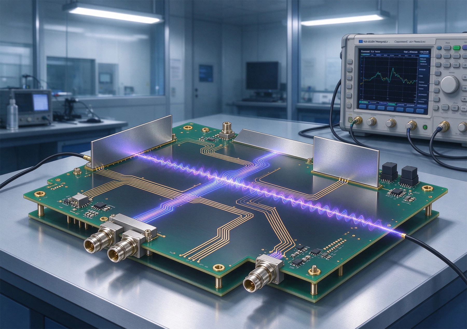
A PCB material is not merely a structural substrate at high frequencies—it is an active participant in the electrical behavior of the system. At low frequencies, the dielectric properties of Fr-4 laminate are approximately constant, and the primary design concerns are Impedance Matching and crosstalk between adjacent traces. At gigahertz frequencies, the story changes completely. The Dielectric Constant of the laminate—the property that determines how fast signals propagate through the material—becomes frequency-dependent in a way that cannot be ignored. A trace on FR-4 that is designed for 50 ohms impedance at one gigahertz may deviate significantly from that target at ten gigahertz, and at the frequencies where high frequency PCBs operate, these deviations are large enough to cause system failure.
Dissipation Factor, or loss tangent, is the other material property that separates high frequency performance from the behavior designers experience at lower frequencies. Every dielectric material converts some portion of the electromagnetic energy passing through it into heat, and the rate of this conversion—the Dissipation Factor—determines how much signal is lost as it travels along a Transmission Line. At low frequencies, this loss is negligible compared to the resistance losses in the conductor itself. At microwave frequencies, dielectric loss can dominate total Insertion Loss, and the difference between a low-loss high-frequency material and standard FR-4 can mean the difference between a link budget that closes and one that falls short by several decibels.
The Skin Effect compounds these material challenges. As frequency increases, alternating current tends to flow on the surface of a conductor rather than uniformly through its cross-section. This concentrates current in a progressively thinner layer near the conductor surface, increasing effective resistance and causing additional losses that scale with frequency. high frequency PCB design must account for Skin Effect losses in conductor design, choosing surface finishes and trace geometries that minimize the impact of this phenomenon on Signal Integrity.
A high frequency PCB is a printed circuit board constructed from Dielectric Materials specifically engineered to maintain stable electrical properties at radio frequency and microwave signal frequencies, typically from approximately one gigahertz upward into the tens or hundreds of gigahertz. The defining characteristic is not a single property but a combination of properties: stable Dielectric Constant across frequency and temperature, low dissipation factor to minimize signal attenuation, consistent material characteristics across production lots, and predictable performance that can be modeled accurately during the design phase.
The frequency threshold that triggers high frequency material requirements varies by application and by how much performance margin your system has. As a practical guideline, designs operating above approximately one gigahertz begin to encounter the performance limits of standard FR-4 materials, and applications above three gigahertz almost universally require specialized high-frequency laminates. Radar systems at C-band and X-band, automotive 77 GHz collision avoidance sensors, 5G millimeter-wave radio units, and Satellite Communications links all operate in frequency ranges where only purpose-engineered materials can deliver the required signal fidelity.
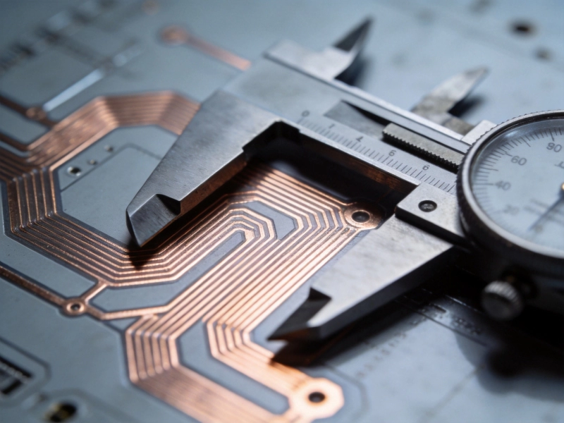
High frequency PCBs are distinguished not just by their materials but by their construction. The tolerances on trace width, dielectric thickness, and Impedance Control are tighter than for standard boards because small variations in these dimensions produce proportionally larger electrical deviations at high frequencies. Via structures introduce discontinuities that must be managed carefully because their parasitic inductance and capacitance become significant relative to the trace impedances they connect. The design practices and fabrication requirements for high frequency boards are correspondingly more demanding than for conventional digital designs.
Dielectric constant stability is the most critical material property for high frequency pcb applications. Standard FR-4 exhibits dielectric constant variation with frequency, temperature, and humidity that is acceptable for digital designs operating below one gigahertz but unacceptable for RF applications where phase stability and impedance predictability are paramount. High Frequency Materials from specialized manufacturers are engineered to maintain dielectric constant within tight tolerances across the frequency range of interest, across the operating temperature range, and across production lots so that designs modeled in simulation behave as predicted when the boards are fabricated.
The dielectric constant itself—the value of Dk in the material specification—varies significantly between material families. Ptfe-based materials, commonly known by the brand name Rogers, offer the lowest dielectric constants in the range of 2.1 to 3.0 and the lowest dissipation factors, but they are expensive, difficult to fabricate using standard PCB processes, and require specialized drilling and plating techniques. Ceramic-filled hydrocarbon materials provide a middle ground with dielectric constants typically ranging from 3.0 to 4.5, dissipation factors significantly lower than FR-4, and fabrication processes closer to standard PCB methods. The selection among these material families involves tradeoffs between electrical performance, cost, and manufacturability that depend on the specific requirements of the application.
Dissipation factor directly determines Signal Loss per unit length in a Transmission Line, and for high frequency applications where every decibel of loss matters, this parameter drives material selection. Standard FR-4 dissipation factor of approximately 0.020 at one gigahertz produces significantly more Signal Loss than high-frequency alternatives that achieve 0.004 or lower. For long Transmission Lines or high-frequency paths where loss accumulates, the difference between a 0.004 Df material and a 0.020 Df material can be decisive for whether the receiver sensitivity requirement is met.
Radar systems of every type—automotive collision avoidance radar, weather surveillance radar, military targeting systems, and aerospace navigation—operate at frequencies where high frequency PCBs are not optional. Automotive 77 GHz radar modules, for example, require board materials that can support millimeter-wave signal propagation with minimal loss and phase distortion. The antennas that transmit and receive these signals are often fabricated as PCB structures using the same high-frequency material as the rest of the module, integrating radiating elements with feed networks and receiver circuitry on a single substrate optimized for RF performance.
Wireless communication infrastructure, particularly the expanding 5G networks deployed at sub-6 GHz and millimeter-wave frequencies, drives substantial demand for high frequency PCBs in base station equipment, active antenna systems, and customer premises equipment. The Massive MIMO architectures used in 5G require RF frontend modules that operate across multiple frequency bands simultaneously, demanding materials that maintain consistent performance over wide frequency ranges and across the temperature extremes encountered in outdoor equipment deployments.
Satellite communications and aerospace systems represent the most demanding applications for high frequency PCBs. Space-qualified electronics must operate in environments where thermal cycling between sunlight and shadow creates extreme temperature swings, where radiation exposure degrades material properties over time, and where failure is not an option. The materials used in these applications undergo extensive qualification testing and must meet military and aerospace specifications that go well beyond the requirements of commercial high frequency applications.
Test and measurement equipment including network analyzers, spectrum analyzers, and signal generators must deliver calibrated accuracy that depends on the signal path materials maintaining predictable, stable electrical properties. These instruments represent some of the most demanding applications for high frequency pcb materials because the calibration accuracy of the instrument depends directly on the consistency of its RF signal paths with the modeled behavior used during calibration.
Ptfe-based materials, pioneered and refined by Rogers Corporation and now available from several manufacturers, represent the highest-performance category for high frequency PCBs. These materials deliver the lowest dissipation factors—often below 0.002 at ten gigahertz—and the most stable dielectric constant across frequency and temperature. The tradeoff is cost and manufacturability. PTFE is difficult to process using standard PCB Fabrication equipment because it does not bond well with conventional prepreg systems and requires specialized surface preparation and drilling techniques. Boards using PTFE materials cost significantly more than equivalent boards on ceramic-filled hydrocarbons, and not all PCB fabricators have the capability to process these materials reliably.
Ceramic-filled hydrocarbon materials, available from Isola, Shengyi, and other laminate manufacturers, provide a practical compromise between performance and manufacturing accessibility. Dissipation factors in the range of 0.003 to 0.006 at ten gigahertz are substantially better than FR-4 and adequate for many commercial high frequency applications including 5G infrastructure, Automotive Radar modules, and point-to-point wireless links. These materials process more like standard Pcb Materials than PTFE, though they still require attention to specific handling and fabrication requirements that differ from conventional FR-4.
Polyimide and specialty epoxy materials fill the space between standard FR-4 and dedicated high-frequency laminates. These materials offer improved thermal performance and better high-frequency properties than general-purpose FR-4 while remaining more affordable than PTFE-based options. For applications that operate above one gigahertz but below the most demanding frequency ranges, these materials often provide the best combination of cost, performance, and fabrication accessibility.
Impedance Control in high frequency PCBs demands tighter tolerances on every dimension that affects trace impedance—trace width, dielectric thickness, and the effective dielectric constant of the material stackup surrounding the trace. Where a standard digital board might specify impedance tolerance of plus or minus ten percent, a high frequency design may require plus or minus five percent or tighter. This tighter tolerance flows back to the fabrication facility, requiring more precise dielectric thickness control, careful management of trace etching to maintain width consistency, and often statistical verification of impedance on production boards rather than testing a single sample from each panel.
Via design requires particular attention in high frequency circuits because vias introduce discontinuities that degrade signal quality. Through-hole vias act as inductive stubs that create resonance effects at high frequencies, and the parasitic capacitance between the via barrel and adjacent planes can create impedance mismatches that produce reflections. Back-drilling—removing the unused portion of the barrel beyond the signal layer—eliminates the stub effect for routed-through signals. Blind and buried vias reduce the number of discontinuities by connecting only the layers that carry the signal. These fabrication options add cost but measurably improve high frequency performance, and the decision to use them should be driven by the Signal Integrity requirements of the specific design.
Ground Plane integrity is more critical at high frequencies than in conventional digital design. Return currents for high frequency signals follow the path of minimum impedance—which is the path directly beneath the signal trace on the nearest reference plane—and any break, slot, or via antipad that interrupts this return path forces the current to take a longer route, creating parasitic inductance and radiatingEMI. High Frequency Pcb layout should maintain continuous reference planes under all critical signal traces and minimize the use of slots, splits, or antipads that would interrupt the Return Current path.
High frequency PCBs cost more than standard boards, and the cost premium is driven by the materials themselves, the specialized fabrication processes required, and the tighter tolerances that inspection and testing demand. PTFE-based boards in particular can cost two to five times as much as equivalent FR-4 boards, and the fabrication process often takes longer because these materials require different drilling parameters, specialized plating processes, and sometimes manual handling that extends the production cycle. These cost and lead time impacts should be factored into project planning early, before design decisions lock in material choices that drive up the total production cost.
The choice of material should be driven by actual requirements rather than assumed to require the highest-performance option available. A design that operates at five gigahertz can often be implemented successfully on a ceramic-filled hydrocarbon material at a fraction of the cost of a PTFE board. Reserve PTFE and other ultra-high-performance materials for applications where the frequency, the loss budget, or the environmental requirements genuinely demand them. Material selection should be a deliberate engineering decision informed by simulation, not a default to the most expensive option.
Fabricator selection is as important for high frequency boards as material selection. Not all PCB manufacturers have the equipment, process knowledge, and quality systems to produce high frequency boards reliably. Working with a fabricator who has demonstrated experience with your chosen material and your specific frequency range—and who can provide impedance testing data, cross-section analysis, and other verification documentation—substantially reduces the risk that the fabricated boards will not match the modeled performance your design was based on.
At what frequency does standard FR-4 stop being suitable for my design?
Above approximately one gigahertz, FR-4's frequency-dependent dielectric properties begin to introduce performance limitations that matter for most applications. Above three gigahertz, FR-4 is generally unsuitable for designs where impedance accuracy, phase stability, or Insertion Loss are critical parameters.
Can I use High Frequency Materials for a mixed-signal board that has both RF and digital sections?
Yes, many high frequency materials work well for mixed-signal designs. The challenge is managing the interface between the RF and digital sections to prevent digital switching noise from coupling into the RF paths. Careful partitioning, Ground Plane management, and filtering at the interface address this concern.
How does temperature affect high frequency PCB performance?
Temperature changes the dielectric constant of the laminate material, which shifts the effective impedance of traces and the phase velocity of propagating signals. High frequency materials are engineered to minimize this temperature dependence, and the temperature coefficient of dielectric constant—measured in parts per million per degree Celsius—is a key specification to evaluate when selecting a material for thermally demanding applications.
Are high frequency PCBs more difficult to fabricate than standard boards?
PTFE-based boards require specialized fabrication processes that not all manufacturers can perform. Ceramic-filled hydrocarbon materials are closer to standard FR-4 in their fabrication requirements, though they still demand attention to specific handling and processing parameters. Working with a fabricator experienced in your chosen material is the most important factor in achieving successful results.
What testing should I expect for high frequency PCBs from the fabricator?
Expect impedance testing of representative samples from each production panel, dielectric constant verification through cross-section analysis, and loss tangent characterization where the application requires it. For demanding applications, time-domain reflectometry traces and S-parameter measurements provide additional verification of the fabricated board's high frequency performance.
Contact us to discuss your requirements and learn how our expertise in High Frequency Pcb Materials and fabrication supports your RF and microwave design objectives.
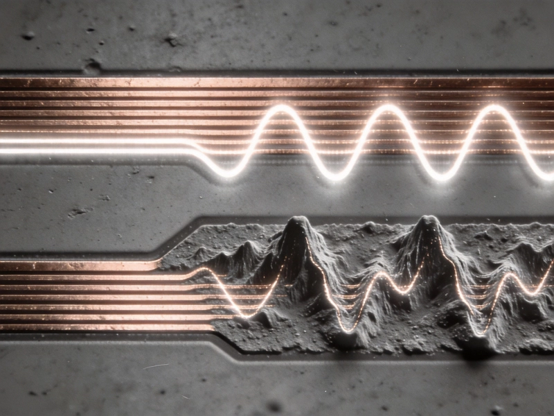
The Impact of Surface Roughness on High Frequency PCB Fabrication QualityJune/27/2026
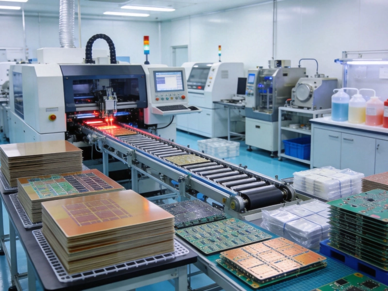
Advanced High Frequency PCB Fabrication Techniques for Low Loss PerformanceMay/29/2026
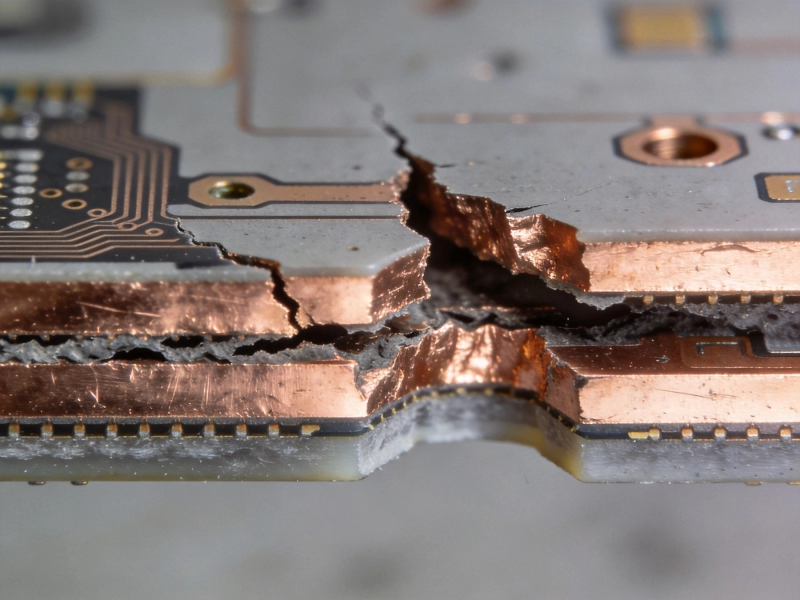
Overcoming Delamination Challenges in Multilayer High Frequency PCB FabricationJuly/28/2026
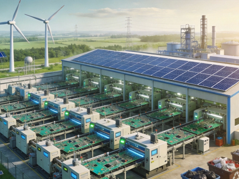
Environmental Considerations in Sustainable High Frequency PCB FabricationSeptember/23/2026
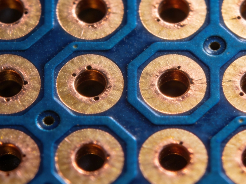
Laser Drilling and Microvias in Modern High Frequency PCB FabricationJuly/07/2026
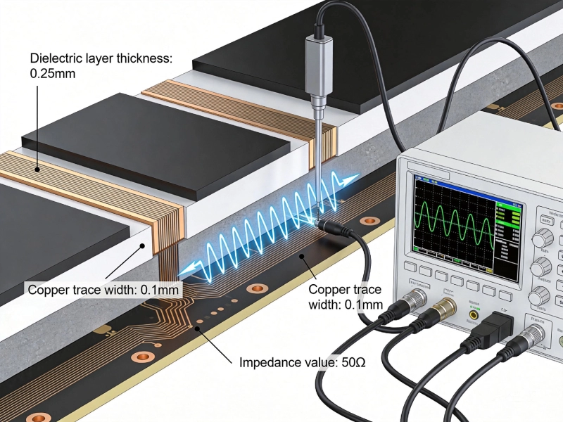
High Frequency PCB Fabrication: Managing Dielectric Constant (Dk) TolerancesJune/09/2026
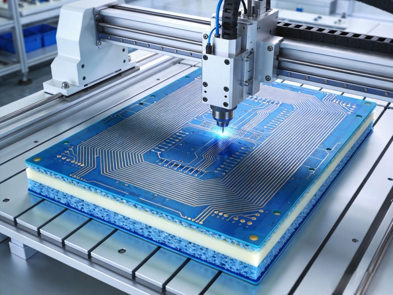
High Frequency PCB Fabrication with Rogers and PTFE Materials: A Technical GuideJuly/16/2026
High Frequency PCB Fabrication Tolerances: Why Precision Matters More Than EverSeptember/02/2026