Open Nav

Among electronics design engineers and PCB procurement specialists, the terms high frequency and high speed are often used interchangeably, as though they describe the same challenge and the same solution. They do not. High frequency PCBs and high speed PCBs address fundamentally different engineering problems, require different material properties, follow different design rules, and are manufactured by different subsets of the PCB industry. Confusing these two categories leads to specification errors, manufacturing problems, and products that fail to meet performance requirements in unexpected ways. Understanding the distinction clearly, and knowing when each technology applies, is essential for anyone involved in designing or sourcing advanced electronic systems.
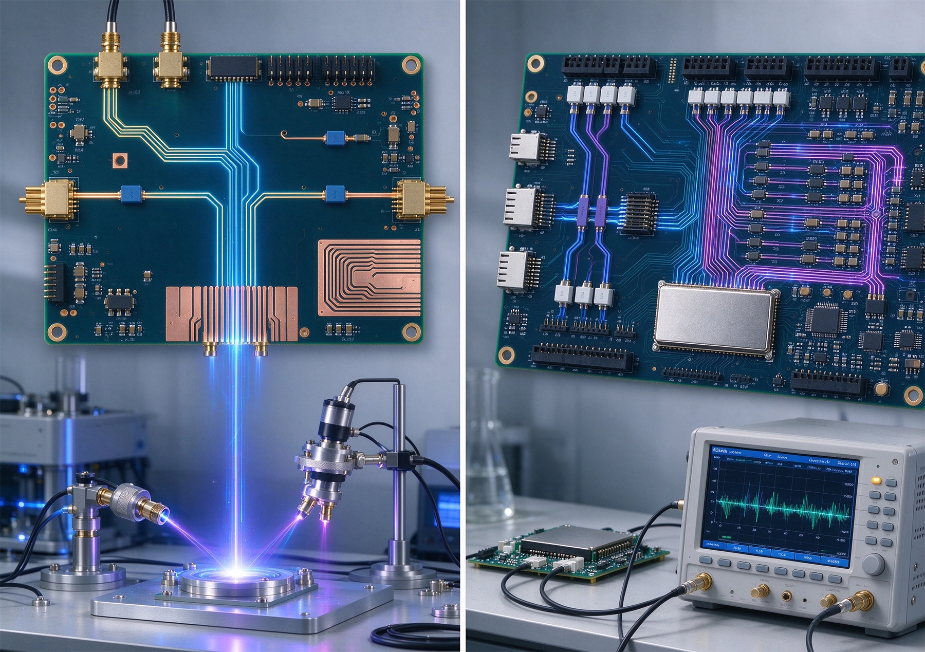
The most important thing to understand is that high frequency and high speed refer to different physical phenomena, even though both involve fast-changing electrical signals. Mixing them up is like confusing the temperature of an oven with the amount of time food spends inside it. Both matter for cooking, but they are not the same thing.
High frequency PCBs are designed for applications where the actual frequency of the signal, measured in megahertz or gigahertz, places specific demands on the electrical properties of the board. A 77 GHz Automotive Radar transceiver, a 5G millimeter-wave front end, and an L-band satellite communication front end all operate at frequencies where the wavelength of the signal approaches the physical dimensions of the traces on the board. At these frequencies, the board material itself becomes part of the circuit, and controlling its electrical properties is critical for proper antenna matching, filter performance, and signal transmission. In high frequency applications, signal propagation delay and wavelength are the primary concerns.
High speed PCBs are designed for applications where the edge rate of digital signals, measured in volts per nanosecond, creates Signal Integrity Challenges even if the fundamental clock frequency is modest. A 100BASE-TX Ethernet transceiver running at 125 MHz or a PCIe Gen3 link at 8 GT/s per lane both qualify as high speed digital designs because the fast signal edges contain frequency components in the gigahertz range that couple into adjacent traces, reflect at impedance discontinuities, and create electromagnetic radiation that interferes with other circuits. In high speed digital applications, signal edge fidelity and timing margin are the primary concerns.
High frequency and high speed applications impose different priorities for the electrical properties of the PCB, which leads to different material and design requirements.
In high frequency analog applications, the most critical electrical properties are Dielectric Constant, loss tangent, and how these properties vary with frequency and temperature. The Dielectric Constant determines the wavelength of signals propagating through the material, which directly affects the electrical length of Transmission Lines and the resonant frequency of distributed circuits like filters and couplers. If the dielectric constant is not tightly controlled and consistent, circuits will not perform as designed. Loss tangent, which quantifies how much signal energy is dissipated as heat in the dielectric, determines Insertion Loss in Transmission Lines and Q factor in resonant structures. At 28 GHz or 77 GHz, even small differences in loss tangent make a measurable difference in system performance.
In high speed digital applications, the most critical electrical properties are Impedance Control, dispersion, and the consistency of these properties across frequency and manufacturing variations. The Characteristic Impedance of transmission lines must match the source and load impedance to prevent reflections that distort signal edges and reduce timing margin. Dispersion, the frequency-dependent variation in propagation velocity, causes different frequency components of a fast digital edge to travel at slightly different speeds, smearing the edge and reducing signal fidelity. While loss is not irrelevant in high speed digital applications, it is typically less critical than impedance and dispersion control, because digital signals are more tolerant of moderate Insertion Loss than narrowband analog circuits are.
The material properties required for high frequency and high speed applications overlap partially but have important differences in emphasis and specification approach.
high frequency PCB materials are typically specified by their dielectric constant at the specific frequency of operation and their loss tangent at that frequency. Common materials include Rogers RT/duroid series with dielectric constants around 2.1 to 10.2, hydrocarbon ceramic laminates like Rogers Ro4003c with a dielectric constant around 3.4, and Ptfe-based materials for the lowest loss applications. The dielectric constant of these materials is relatively stable across frequency, meaning that performance modeled at one frequency closely predicts performance at nearby frequencies. This predictability is essential for designing distributed circuits like filters and couplers that depend on precise wavelength relationships.
High speed digital Pcb Materials are most commonly based on standard FR4 or enhanced FR4 systems, because the primary concern is impedance consistency rather than absolute dielectric constant values. The dielectric constant matters primarily for ensuring consistent 50-ohm or 100-ohm impedance across traces and over temperature. Materials like Panasonic Megtron 6, Isola I-tera, and Rogers 3003 offer lower loss than standard FR4 while maintaining the processing characteristics that make them compatible with standard Pcb Manufacturing. For the highest speed digital applications above 25 GT/s, Low-loss Materials become more important and Ptfe-based or hydrocarbon ceramic materials may be appropriate, blurring the line between high speed digital and high frequency analog requirements.
The coefficient of thermal expansion of the dielectric material affects both categories differently. In high frequency applications, thermal expansion changes the physical dimensions of transmission lines, shifting the electrical length and resonant frequency of circuits. This drift can be significant for outdoor equipment subject to wide temperature ranges. In high speed digital applications, thermal expansion affects via stub lengths and the consistency of differential pair spacing, which can degrade Signal Integrity at very high speeds.
The layout and routing rules that apply to high frequency and high speed PCBs reflect their different performance priorities, and applying the wrong set of rules leads to design errors that are expensive to fix.
high frequency PCB design focuses on controlling Transmission Line geometry to achieve precise Characteristic Impedance and on managing wavelength-related effects like reflection, radiation, and coupling. Microstrip and Grounded Coplanar Waveguide are the most common Transmission Line types, with geometry chosen to achieve the target impedance and to minimize radiation loss. Stripline is used when Shielding from external interference is critical. Trace width and spacing tolerances of a few microns may be required for critical circuits, and manufacturing capability must be verified to meet these tolerances consistently. Ground Plane integrity is critical because gaps or slots in the ground reference create impedance discontinuities and mode conversion that degrade performance.
High speed digital PCB design focuses on controlling impedance consistency, minimizing crosstalk between adjacent signal traces, and maintaining signal return path integrity. Differential pair routing with controlled differential impedance is common for Serializer/Deserializer based links, with tight coupling requirements that must be maintained through bends and connectors. Length matching within tight tolerances ensures that differential signals arrive at the receiver simultaneously, preserving the timing margin built into the system architecture. Via design must minimize stub length that creates resonance at signal frequencies, often requiring back-drilling or blind/buried via construction to remove the unused portion of through vias.
high frequency pcb technology is the appropriate choice when your application involves analog signal transmission at radio frequencies where wavelength effects dominate circuit behavior. Several categories of applications clearly fall into this category.
Wireless communication systems operating above 6 GHz fall squarely in the high frequency domain. 5G millimeter-wave base station equipment at 28 GHz and 39 GHz, satellite communication systems at L-band through Ka-band, and point-to-point microwave links at 24 GHz all require High Frequency Materials and design techniques to achieve acceptable antenna feed network performance, filter selectivity, and low-noise amplifier design. The distributed nature of these circuits, where transmission line lengths are a significant fraction of the signal wavelength, demands precise control of dielectric properties and geometry that only specialized High Frequency Materials can provide.
Automotive Radar systems at 77 GHz and 79 GHz represent one of the most demanding high frequency applications in volume production today. The short wavelength of these signals creates antenna arrays that fit on a single PCB, but the tight wavelength relationships required for proper beamforming demand exceptional consistency in dielectric constant and trace geometry across the entire antenna array. Material selection and Manufacturing Quality control at this frequency are extraordinarily demanding, and only a few manufacturers worldwide can produce these boards at volume with the required consistency.
Radar and sensing systems for industrial, aerospace, and defense applications frequently operate at high frequencies where the ability to create compact, wavelength-appropriate transmission line circuits is essential. Weather radar at C-band and X-band, aircraft collision avoidance systems, and industrial level measurement systems all require high frequency pcb technology to achieve the required performance in compact, lightweight packages.
High speed PCB technology is the appropriate choice when your application involves fast digital signals where edge fidelity and timing integrity are the primary concerns. Many modern digital systems fall into this category.
Data center networking equipment including switches, routers, and interface cards uses high speed digital PCB technology for 10GbE, 25GbE, 100GbE, and emerging 400GbE interfaces. These systems operate at clock rates up to 56 GHz per lane while maintaining strict jitter and eye diagram requirements that demand careful attention to Impedance Control, differential pair routing, and via design. Standard high-Tg FR4 materials with good process consistency are typically adequate for these applications, but design rules must be followed precisely to achieve the required Signal Integrity.
High performance computing boards including GPUs, FPGAs, and ASIC carrier boards use high speed digital PCB technology for the massive parallel interfaces that connect chips at data rates of 25 to 56 GT/s per lane. These applications push the limits of PCB technology, requiring very Low-loss Materials, extremely tight impedance tolerance, and sophisticated via design to maintain signal quality across hundreds of high-speed links on a single board. While the signals are digital, the frequencies involved approach those of high frequency analog applications, and material selection begins to overlap between the two categories.
Consumer electronics with high-speed interfaces including USB4, Thunderbolt 4, and HDMI 2.1 also require high speed PCB technology, though at lower data rates and with less stringent requirements than enterprise computing applications. Cost optimization is more important in these applications, and standard manufacturing approaches with enhanced materials often provide the right balance of performance and cost.
In practice, many applications involve both high frequency and high speed concerns simultaneously, creating design challenges that require attention to both categories of requirements.
Software-defined radio platforms that digitize signals directly at radio frequencies illustrate this overlap clearly. These systems use high frequency analog front ends to down-convert RF signals to intermediate frequencies or to baseband, then process those signals with high speed analog-to-digital converters and digital signal processors. The analog front end requires high frequency materials and design techniques, while the digital processing backplane requires high speed digital techniques. The transition between these two domains, typically at the ADC or DAC, must satisfy both sets of requirements simultaneously.
Automotive radar systems with digital beamforming create similar overlap. The antenna array operates at 77 GHz and requires high frequency design techniques, but the digital processing that forms the beam uses high speed digital interfaces to route data between the antenna module and the processing electronics. Boards that span both domains must address material selection, stack-up design, and manufacturing requirements for both high frequency and high speed performance.
5G baseband units that process signals at intermediate frequencies also span the boundary between high frequency and high speed. The radio unit at the antenna may use high frequency materials for the RF front end, while the baseband processing unit uses high speed digital materials for the data processing interfaces. Designing boards that transition between these two domains requires careful planning of the stack-up, routing, and material transitions to avoid performance degradation at the interface.
High frequency and high speed PCBs have different manufacturing requirements that affect sourcing strategy and supplier selection.
High frequency Pcb Manufacturing requires specialized equipment and process expertise that not all PCB manufacturers possess. Laser drilling for microvias, Controlled Impedance testing with time-domain reflectometry or vector network analysis, and specialized lamination processes for low-loss materials require significant capital investment and technical expertise. Manufacturers who specialize in high frequency applications often serve aerospace, defense, and automotive radar markets, and their pricing reflects the precision and consistency these demanding applications require.
High speed digital PCB manufacturing is more widely available, with many manufacturers offering Controlled Impedance testing and enhanced FR4 materials as standard capabilities. For the most demanding high speed applications above 25 GT/s, the requirements for low-loss materials and tight impedance tolerance approach those of High Frequency Manufacturing, and specialist manufacturers become necessary. For more moderate high speed requirements, a broader range of manufacturers can meet the requirements, creating more competitive pricing and shorter lead times.
Verification testing requirements differ between the two categories. High frequency boards are typically verified with vector network analysis that measures S-parameters and confirms impedance, insertion loss, and return loss at the frequencies of interest. High speed boards are typically verified with time-domain reflectometry for impedance and eye diagram testing for signal integrity. Understanding what verification testing is appropriate for your application ensures you receive the documentation and test data you need to confirm your boards meet specifications.
High frequency and high speed PCBs serve different purposes and require different approaches, even though both deal with fast signals. High frequency technology is the right choice for analog applications where signal wavelength and dielectric properties determine circuit performance. High speed technology is the right choice for digital applications where signal edge fidelity and timing integrity determine system performance. Understanding which category applies to your application, and selecting materials and manufacturers accordingly, leads to designs that meet performance requirements without over-specifying and over-paying for capability you do not need.
The gray areas where both considerations apply are growing as systems become more integrated and as digital data rates continue to increase. Staying current with the evolving boundary between high frequency and high speed requirements helps engineering teams make appropriate design choices and avoid costly mistakes from applying the wrong set of rules to their application.
When specifying requirements for either high frequency or high speed applications, clear communication with your manufacturer about the actual application, frequencies involved, and performance requirements ensures they can recommend the most appropriate materials and manufacturing approach for your specific needs.
Contact us to discuss your requirements and explore whether high frequency or high speed PCB technology is the right choice for your application.
High Frequency PCB Knowledge: How to Minimize Insertion Loss and ReflectionJuly/21/2026
Key High Frequency PCB Knowledge for Successful RF Circuit DesignSeptember/07/2026
Advanced High Frequency PCB Knowledge: Using Simulation Tools for Better ResultsSeptember/29/2026
Essential High Frequency PCB Knowledge for Hardware Engineers and DesignersMay/29/2026
Demystifying Impedance Control: Core High Frequency PCB KnowledgeJuly/09/2026
Essential High Frequency PCB Knowledge for Hardware Engineers and DesignersJune/15/2026
The Engineer's Guide to High Frequency PCB Knowledge and Stack-up DesignJuly/31/2026
High Frequency PCB Knowledge: Managing Crosstalk and EMI in Dense LayoutsAugust/11/2026