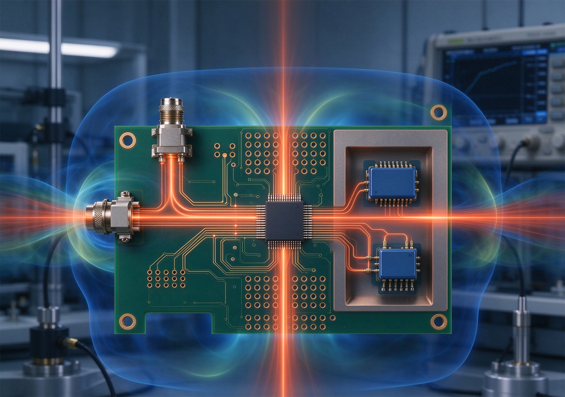
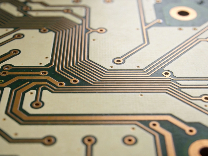
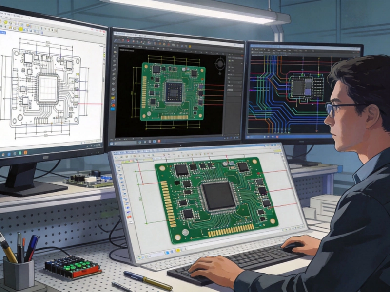
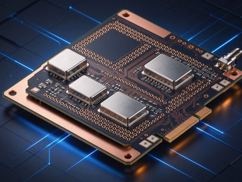
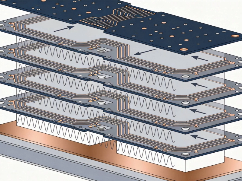
High frequency and radio frequency (RF) circuits—used in 5G communications, radar systems, satellite links, medical devices, and millimeter-wave applications—are extremely sensitive to PCB design choices. Even minor design errors that would have no impact on low-frequency digital circuits can cause severe signal degradation, increased noise, reduced range, or complete circuit failure at RF frequencies. Achieving stable, predictable RF performance requires following specialized design guidelines from the earliest schematic stage through to manufacturing. When implemented correctly, these guidelines can reduce Signal Loss by 30-50%, improve receiver sensitivity by 6-10dB, and ensure consistent performance across temperature and operating conditions.

Core Challenges of High Frequency PCB Design
At frequencies above 1GHz (and especially above 10GHz for millimeter-wave applications), conventional PCB design rules no longer apply, as electromagnetic effects dominate circuit behavior:
- Signal attenuation (Insertion Loss): High frequency signals lose significantly more power as they travel through PCB traces and materials, with losses increasing exponentially with frequency. A trace that has 0.1dB loss at 1GHz may have 3dB or more loss at 40GHz, cutting effective signal power in half.
- Signal Reflection: Impedance mismatches as small as 10% can cause 20% or more of the signal to be reflected back to the source, reducing effective output power, increasing voltage standing wave ratio (VSWR), and causing signal distortion.
- Crosstalk and Emi: High frequency signals radiate much more readily than low-frequency signals, leading to increased crosstalk between adjacent traces, Electromagnetic Interference (Emi) with other circuits, and susceptibility to external noise sources.
- Tight impedance tolerance requirements: Most RF systems require Controlled Impedance with ±5% tolerance (and even ±2% for high-performance millimeter-wave applications), far tighter than the ±10% tolerance acceptable for low-frequency digital circuits.
- Thermal drift: Changes in temperature cause variations in substrate Dielectric Constant (Dk) and trace dimensions, leading to impedance shifts and performance drift that can take Rf Circuits out of specification over their operating temperature range.
1. Material Selection: The Foundation of RF Performance
Your choice of Pcb Materials is the single most important factor in achieving stable RF performance. Standard Fr-4 materials are only suitable for applications below 1GHz; for higher frequencies, you need specialized high-frequency laminates:
Key Material Parameters to Consider:
- Low, stable Dielectric Constant (Dk): Choose materials with a Dk value that is consistent across your operating frequency range and temperature range. For most RF applications, Dk values between 2.2 and 3.5 are preferred, as they provide a good balance between Impedance Control and trace width. Look for materials with Dk tolerance of ±0.05 or better to ensure consistent impedance across production lots.
- Low Dissipation Factor (Df): Df measures how much energy the material absorbs from the signal, directly contributing to Insertion Loss. For applications above 10GHz, choose materials with Df ≤ 0.004 at your operating frequency; for millimeter-wave applications above 30GHz, look for Df ≤ 0.002.
- Low copper roughness: High frequency signals travel primarily on the surface of copper traces (Skin Effect), so rough copper surfaces significantly increase insertion loss. For frequencies above 10GHz, use low-profile or reverse-treated copper foils with roughness <0.5μm Ra to minimize loss. Standard electrodeposited copper with 2μm roughness can increase loss by 30% or more at 40GHz.
- Thermal stability: Select materials with a high Glass Transition Temperature (Tg > 170°C) and low coefficient of thermal expansion (CTE) matched to copper, to minimize dimensional changes and Dk drift over temperature. For high-power RF applications, choose materials with high thermal conductivity to improve heat dissipation.
Recommended Materials by Frequency Range:
- 1-6 GHz: Mid-range Fr-4 (high Tg, controlled Dk) or Rogers Ro4003c for better performance
- 6-24 GHz: Rogers Ro4350b, Arlon AD255, or Taconic Rf-35
- 24-100 GHz (millimeter-wave): Rogers RO3003, RO3006, or ceramic-filled Ptfe materials with very low Df
For cost-sensitive designs, consider hybrid stackups that use high-frequency materials only for critical RF layers, with standard FR-4 for digital and power layers to reduce overall cost.
2. Stackup Design and Impedance Control
A carefully designed stackup is critical for achieving Controlled Impedance, minimizing loss, and reducing EMI in high frequency designs:
- Always provide a continuous reference plane: Every high frequency signal layer must be adjacent to a solid ground (preferred) or power reference plane to form controlled-impedance Microstrip or stripline structures. Never route high frequency signals without an adjacent reference plane, as this leads to uncontrolled impedance, increased radiation, and high crosstalk.
- Minimize dielectric thickness between signal and reference plane: For Microstrip lines, thinner dielectric layers reduce radiation and crosstalk, improve Impedance Control, and allow narrower trace widths for a given impedance. For 50Ω impedance on Rogers Ro4350b (Dk=3.48), a 0.1mm dielectric thickness requires a 0.18mm trace width, while a 0.5mm dielectric requires a 0.85mm trace width, which takes more space and is more prone to crosstalk.
- Use professional impedance calculation tools: Never rely on rule-of-thumb impedance calculations. Use specialized tools like Polar SI9000 or ANSYS SIwave to calculate trace widths and stackup dimensions based on your actual material properties, copper thickness, and operating frequency. Always include a 10% design margin to account for manufacturing tolerances.
- Separate RF, analog, and digital sections: In mixed-signal designs, use separate stackup regions or isolation planes for RF, analog, and digital circuits to prevent noise coupling. Keep high-speed digital layers as far as possible from RF layers, with ground planes in between for isolation.
- Pair power and ground planes: Place power planes adjacent to ground planes to form low-inductance capacitance that reduces power supply noise, which is critical for low-noise RF amplifier and receiver circuits.
Differential Pair Design Rules:
For differential RF interfaces (like LVDS, USB 3.0, or millimeter-wave differential signals):
- Maintain constant spacing between differential pairs along their entire length to ensure consistent differential impedance
- Match pair lengths to within 1/20 of the signal wavelength at your operating frequency to minimize phase mismatch
- Route differential pairs symmetrically, avoiding asymmetric bends or topology changes that would cause impedance imbalance
- Use the same reference plane for both lines in the differential pair to avoid common-mode noise issues
3. Routing Best Practices for High Frequency Signals
Even with the right materials and stackup, poor routing can destroy RF performance. Follow these routing guidelines:
- Minimize trace length: Keep high frequency signal traces as short as possible to reduce insertion loss and phase delay. For critical RF paths like antenna feeds or power amplifier outputs, prioritize direct routing over aesthetic considerations.
- Avoid 90° bends: Use 45° angles or curved bends for RF traces instead of 90° corners, which cause impedance discontinuities and Signal Reflection. A 90° bend can create a 10-15% impedance mismatch at 30GHz, leading to VSWR > 1.5:1.
- Minimize via usage: Each via introduces approximately 0.3-1dB of insertion loss (depending on frequency) and creates an impedance discontinuity. Avoid using vias in critical RF paths whenever possible. If you must use vias:
- Use back-drilling to remove unused via stubs, which cause resonance and signal reflection at high frequencies
- Add impedance compensation by adjusting trace width near the via
- Surround signal vias with grounded guard vias spaced 1/20 wavelength apart to reduce crosstalk and radiation
- Never cross plane splits: Never route an RF trace across a split or gap in the reference plane, as this causes a large impedance discontinuity, increased radiation, and significant return path inductance. If you must cross a split, use a bridge capacitor or jumper to maintain a continuous return path.
- Provide sufficient isolation between signals: Maintain a spacing of at least 3x the trace width between adjacent RF traces to minimize crosstalk. For high-isolation applications (like separating transmit and receive paths), use grounded copper guard traces with multiple vias along their length, or physical isolation slots in the PCB between sensitive circuits.
- Control stub lengths: Any stub (a short length of trace branching off the main signal path) longer than 1/20 of the signal wavelength will cause resonance and signal degradation. Keep stubs as short as possible, or eliminate them entirely by using series termination or alternative routing.
4. Grounding and Noise Mitigation
Proper Grounding is critical for minimizing noise and ensuring stable RF performance:
- Use solid ground planes: Provide a large, continuous Ground Plane for all Rf Circuits to minimize ground impedance, provide Shielding, and ensure consistent return paths for RF signals. Avoid splitting the Ground Plane unless absolutely necessary.
- Plentiful grounded vias: Add ground vias regularly along RF traces, around shielded areas, and near component ground pads, spaced no more than 1/20 of the signal wavelength apart. This minimizes the inductance of ground connections and reduces common-mode noise.
- Isolate RF and digital grounds: In mixed-signal designs, keep RF and digital ground planes separate, connecting them only at a single point (star ground) or through a ferrite bead to prevent digital switching noise from coupling into sensitive RF circuits.
- Use via fences for isolation: For high-isolation applications (e.g., between transmitter and receiver sections), create a Via Fence along the isolation boundary: a row of grounded vias spaced 1/20 wavelength apart, connected to top and bottom ground planes, to prevent RF energy from propagating between sections.
- Shield sensitive circuits: For extremely sensitive receiver circuits or high-power transmitter circuits, add a metal shield can soldered to the ground plane around the circuit to block EMI and crosstalk. Include plenty of ground vias under the shield mounting pads for a low-inductance connection.
5. Component Placement and Power Distribution
Component Placement and power distribution design have a significant impact on RF performance:
- Minimize path lengths through placement: Place RF components as close together as possible to minimize the length of high-frequency signal paths. Place critical components first: antenna connectors, filters, power amplifiers, and low-noise amplifiers, then route supporting circuits around them.
- Isolate input and output stages: Separate high-power output circuits from low-power input circuits to prevent feedback and oscillation. Place input and output connectors on opposite sides of the board if possible, and route their paths away from each other.
- Proper RF decoupling: Each active RF component (amplifiers, mixers, oscillators) requires multi-stage decoupling at its power pins, placed as close to the pin as possible:
- A 1nF high-frequency ceramic capacitor for VHF/UHF frequencies
- A 0.1μF MLCC capacitor for mid-range frequencies
- A 1-10μF tantalum or ceramic capacitor for low-frequency noise
Use low-ESR (equivalent series resistance) capacitors rated for RF operation, and connect them to ground with short, wide traces and multiple vias to minimize inductance. - Filter power supplies for RF circuits: Isolate RF power rails from digital power rails using LC filters or ferrite beads to prevent digital noise from entering the RF section. Use separate voltage regulators for RF and digital circuits whenever possible.
- Thermal Management: High-power RF components like power amplifiers generate significant heat, which can cause performance drift or component failure. Place these components near the edge of the board for easy heat sinking, and add an array of thermal vias under the component pad to conduct heat to internal ground planes or external heat sinks.
6. Design for Manufacturing and Testing
Even the best design will fail if it cannot be manufactured consistently. Follow these guidelines to ensure your design performs as intended in production:
- Consult your manufacturer early: Discuss your design with your Pcb Manufacturer before finalizing it, to confirm their capability to meet your impedance tolerance, material, and fine-line routing requirements. Get their recommended design rules for high-frequency boards to avoid manufacturing issues.
- Include impedance test coupons: Add impedance test coupons to the panel edge for every controlled impedance layer, so you can verify that the manufactured boards meet your impedance specifications before assembly.
- Add RF test points: Include calibrated RF test points in critical signal paths for testing and debugging. Use 50Ω matched test points with ground pads close by for probe connections, and keep the stub length from the main signal path to the test point as short as possible (≤1/20 wavelength).
- Specify material requirements clearly: On your fabrication drawing, explicitly state the exact material part number, Dk/Df requirements, copper foil type, and impedance tolerance. Do not allow substitutions of lower-grade materials, as this will destroy RF performance.
- Design for temperature performance: Characterize your design's performance across its full operating temperature range during Prototype Testing, to account for Dk drift and component tolerance variations. Include tuning elements (like variable capacitors or trimmer resistors) if you need to adjust performance in production.
Common High Frequency Design Mistakes to Avoid
- Using FR-4 for high-frequency applications: Standard FR-4 has high Df and unstable Dk that varies significantly with frequency and temperature, leading to excessive loss and impedance variation at frequencies above 1GHz.
- Ignoring copper roughness: High copper roughness can increase insertion loss by 30% or more at millimeter-wave frequencies, even if you use a low-Df substrate.
- Long via stubs: Unbackdrilled vias with long stubs are a common cause of resonance and poor performance in multi-layer high-frequency designs. Always specify back-drilling for vias in high-frequency paths.
- Insufficient Grounding: Too few ground vias lead to high ground inductance, increased noise, and poor isolation between circuits.
- Poor impedance calculation: Using generic impedance calculators that don't account for your specific material properties or copper thickness leads to significant impedance errors.
Case Study: 28GHz 5G Millimeter-Wave Module Design Improvement
We recently assisted a customer designing a 28GHz 5G customer premises equipment (CPE) module that was underperforming: measured insertion loss was 3.2dB higher than simulated, and effective communication range was only 40% of the design target.
Our design review identified the following issues:
- The design was using standard FR-4 material for the RF layer, which had 2.8dB higher loss at 28GHz than the intended Rogers RO3003 material
- Via stubs of 0.8mm length were creating resonance at 28GHz, adding an additional 0.9dB loss
- RF traces were crossing a split in the ground plane, causing significant signal reflection
After implementing our recommended design changes:
- Switched to Rogers RO3003 substrate with low-profile copper foil
- Added back-drilling to remove via stubs
- Re-routed RF traces to avoid crossing plane splits, and added guard vias along critical paths
The revised design measured insertion loss just 0.3dB higher than simulation, and communication range improved by 2.2x, exceeding the original design target. The design is now in Mass Production with >98% yield for RF performance.
high frequency PCB design requires careful attention to every aspect of the design process, from material selection and stackup design to routing, grounding, and manufacturing specifications. By following these guidelines and working closely with an experienced High-frequency Pcb Manufacturer, you can achieve stable, predictable RF performance even for the most demanding millimeter-wave applications.
Contact us to discuss your requirements.