Open Nav

high frequency PCB assembly is where theoretical Signal Integrity meets physical reality. Even a perfectly simulated Rf Design can underperform if assembly introduces impedance discontinuities, parasitic reactance, thermal stress, or contamination. As operating frequencies extend into millimeter-wave bands for 5G, Automotive Radar, satellite communication, and high-speed digital interfaces, assembly process control becomes as critical as layout and material selection.
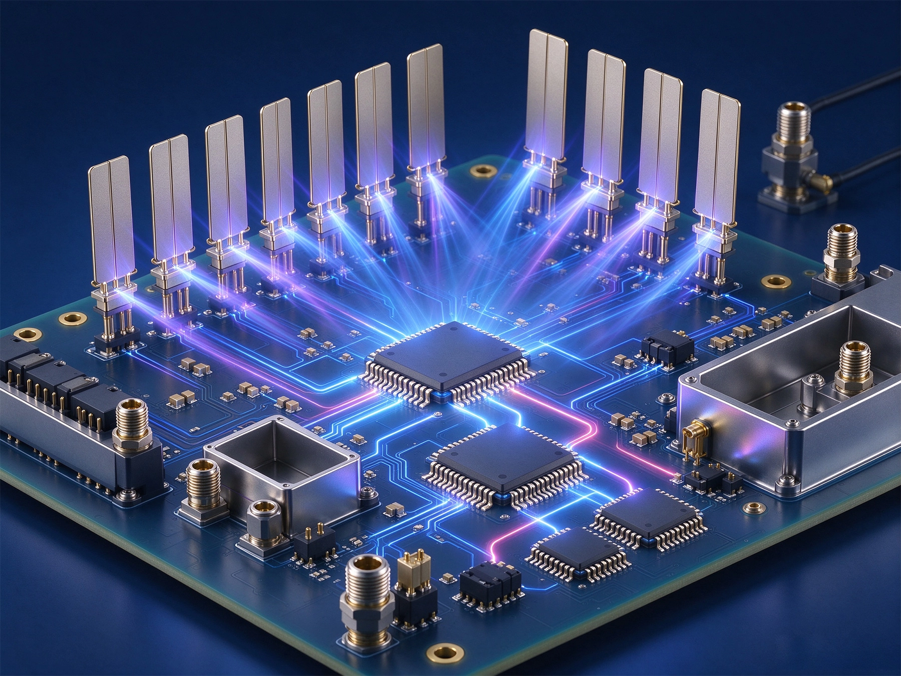
At high frequencies, signal energy concentrates near conductor surfaces due to the Skin Effect, and even small geometric deviations alter impedance. A solder joint that is acceptable on a low-frequency board can introduce enough parasitic capacitance or inductance to shift a matching network, degrade return loss, or reduce Insertion Loss margin. Assembly therefore cannot be treated as a generic back-end process. It must be designed, qualified, and controlled as part of the RF signal path.
High frequency boards commonly use Ptfe-based laminates, ceramic-filled hydrocarbons, and other Low-loss Materials with stable Dielectric Constant (Dk) and low Dissipation Factor (Df). These materials often have higher coefficients of thermal expansion, lower surface energy, and different thermal stability compared with standard Fr-4. Ptfe substrates, for example, can be more prone to Z-axis expansion during reflow, which increases stress on plated through-holes and microvias.
Assembly teams must adapt reflow profiles, support strategies, and handling procedures to the specific laminate system. Using a standard Fr-4 thermal profile on a PTFE or mixed-material stackup can increase the risk of delamination, pad lifting, or via barrel cracking.
High frequency designs often specify ultra-low profile (ULP) or very low profile (VLP) copper to reduce conductor loss. While smooth copper improves RF performance, it can also affect solder wetting and pad adhesion. Stencil design, solder paste chemistry, and reflow atmosphere may need adjustment to maintain reliable joints without compromising surface finish quality or Impedance Control.
Solder paste volume is one of the most sensitive variables in high frequency assembly. Excess paste increases parasitic capacitance, especially under small RF passives and high-density connectors. Insufficient paste increases joint inductance and raises the risk of open connections or weak mechanical attachment.
Best practices include:
Placement accuracy directly affects impedance continuity. At microwave and millimeter-wave frequencies, even small misalignments can change the effective electrical length of a trace, shift resonant frequencies, or disturb differential coupling. High frequency assemblies typically require tighter placement tolerances than conventional consumer electronics boards.
For RF matching components such as 0402, 0201, or smaller packages, pad symmetry and placement centering are critical. Asymmetric pads create uneven wetting forces, which can cause tombstoning or rotate components slightly out of alignment. This is especially problematic in pi-networks, baluns, and antenna feed structures where layout symmetry is part of the electrical design.
Reflow profiles must balance three competing requirements: reliable solder joint formation, minimal thermal stress on the substrate, and controlled warpage during heating and cooling. High frequency laminates may have lower thermal margins than high-Tg FR-4, and mixed-material stackups can expand unevenly across layers.
Recommended practices include:
For assemblies with large RF shields, power amplifiers, or heavy ground planes, preheating and thermal mass distribution must be considered. Large copper areas can act as heat sinks, creating uneven reflow conditions that lead to head-in-pillow defects or insufficient fillet formation.
Every solder joint adds parasitic inductance and capacitance. In low-frequency circuits these effects are often negligible, but at GHz frequencies they can shift filter response, degrade isolation, or reduce amplifier stability. Grounded components such as shunt capacitors and RF shield frames are particularly sensitive because their Grounding path becomes part of the RF return network.
To minimize parasitic effects, designers and assemblers should coordinate pad geometry, stencil apertures, and via placement. Ground pads should have sufficient solder to form a low-inductance connection, but not so much that solder spreads into adjacent signal areas. For RF shield cans, consistent coplanarity and adequate paste volume help ensure continuous Grounding around the entire perimeter.
Connectors such as SMA, SMP, and edge-launch types are common failure points in high frequency assemblies. Poor soldering of the outer ground shell increases ground inductance and degrades return loss, especially above 10 GHz. Best practices include:
RF Shielding is often required to isolate sensitive receivers, synthesizers, and power amplifiers. Shield frames are typically reflow soldered, while covers may be attached later to allow rework access. Because shield frames cover large ground areas, they can disturb reflow uniformity if not properly designed. Thermal relief patterns, adequate paste volume, and coplanarity control help prevent cold joints and intermittent grounding.
Flux residues that are acceptable on low-frequency boards can degrade high frequency performance. Residues may absorb moisture, reduce surface insulation resistance, and alter the effective dielectric environment around Microstrip lines. Above certain frequencies, even small changes in surface permittivity can shift impedance and resonant behavior.
For assemblies operating above 5–10 GHz, post-assembly cleaning is often recommended. Ion contamination testing should be used to verify cleaning effectiveness. If Conformal Coating is required, its Dielectric Constant and thickness must be accounted for in the design, because coating over exposed Transmission Lines changes impedance.
High frequency assemblies require more than visual inspection. Automated optical inspection (AOI) can detect missing components, bridging, and gross misalignment, but it cannot verify RF performance. X-ray Inspection is important for BGAs, QFNs, connector pins, and shielded joints. For critical RF paths, electrical verification should include:
Tdr is especially useful because it reveals localized impedance disturbances caused by excessive solder, insufficient via fill, connector transitions, or damaged hole walls.
Many assembly challenges can be reduced through early design decisions. Designers should work with assembly partners before finalizing footprints, stackups, and panel layouts.
Key Dfm considerations include:
high frequency PCB assembly demands tighter control than conventional electronics manufacturing. Material selection, solder paste printing, placement accuracy, reflow profiling, connector attachment, cleaning, and electrical verification all influence final RF performance. The most reliable results come from treating assembly as an extension of the Rf Design rather than a separate production step.
Successful high frequency assemblies depend on collaboration between design, fabrication, and assembly teams. When process constraints are understood early, engineers can avoid costly redesigns, reduce prototype iterations, and achieve more predictable Signal Integrity at GHz and millimeter-wave frequencies.
High frequency laminates often have different thermal expansion, surface energy, and moisture sensitivity compared with FR-4. Standard reflow profiles and handling methods may cause warpage, delamination, or via stress. Assembly parameters must be matched to the specific substrate system.
Excess solder increases parasitic capacitance, while insufficient solder increases inductance and joint resistance. Both conditions can shift impedance, degrade return loss, and reduce assembly reliability, especially on fine-pitch RF components and high-speed connectors.
AOI and X-ray inspection are essential for defect detection, but electrical verification such as TDR and Vna Testing is often required to confirm RF performance. These tests identify impedance discontinuities that visual inspection cannot reveal.
Cleaning is recommended for assemblies operating at higher GHz frequencies, especially when flux residues remain near exposed Transmission Lines. Residues can absorb moisture and change the local dielectric environment, affecting impedance and loss.
The Challenges of High Frequency PCB Assembly: Handling Sensitive ComponentsMay/29/2026

Why Component Placement is Critical in High Frequency PCB AssemblyJune/25/2026

High Frequency PCB Assembly for Automotive Radar: Precision and ReliabilitySeptember/21/2026

How to Select a Turnkey High Frequency PCB Assembly PartnerAugust/06/2026
SMT vs. THT: Assembly Techniques for High Frequency PCBsJuly/03/2026

Ensuring Signal Integrity During High Frequency PCB Assembly ProcessesJuly/15/2026
High Frequency PCB Assembly Best Practices for 5G and RF ModulesJune/08/2026
Avoiding Soldering Defects in High Frequency PCB Assembly for RF ApplicationsSeptember/11/2026