Open Nav

The demand for high frequency PCBs isn't growing slowly—it's accelerating. 5G infrastructure deployment continues worldwide. Millimeter-wave radar systems are becoming standard in automotive applications. Satellite communication constellations require boards that perform at frequencies that were exotic just a few years ago. IoT devices push into higher bands to avoid congested spectrum. Each of these applications demands PCBs that don't just carry signals, but carry them with minimal loss, Controlled Impedance, and predictable behavior at frequencies where every material property and manufacturing variable matters.
If your current supply chain treats high frequency boards the same way it treats standard digital designs, you're leaving performance on the table—and probably experiencing yield problems, delivery delays, and cost overruns that come from forcing a general-purpose manufacturing process to do specialized work. Upgrading your supply chain with a partner who has invested in dedicated high frequency capabilities isn't just about getting better boards. It's about removing friction from your product development and production.
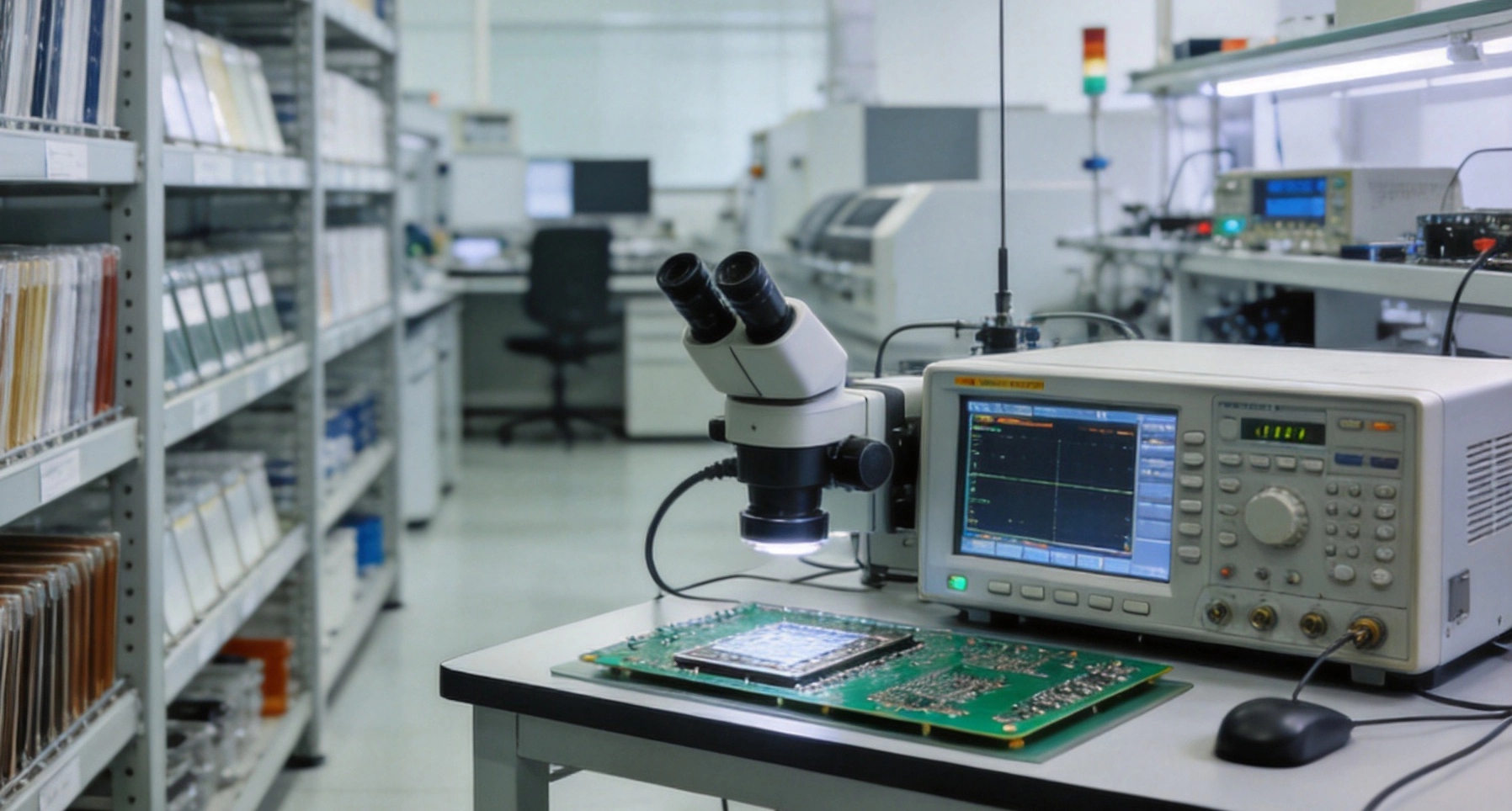
The term "high frequency" gets used loosely. Let's be specific about what it means in a manufacturing context and why it matters.
High frequency PCBs operate at frequencies where the material's dielectric properties—Dielectric Constant (Dk) and Dissipation Factor (Df)—directly affect signal performance. At low frequencies, standard Fr-4 works fine because the material's losses are negligible relative to the signal energy. As frequency increases, Fr-4's relatively high Df (around 0.02 at 10 GHz) causes significant signal attenuation. Boards that need to carry signals above 3 to 5 GHz with low loss require materials with Df values an order of magnitude lower.
Manufacturing these boards is different from manufacturing standard FR-4 boards. The materials process differently—Ptfe-based laminates don't drill the same way as epoxy-glass, and their coefficient of thermal expansion doesn't match standard prepreg. Impedance Control requirements are tighter because high frequency signals are more sensitive to impedance discontinuities. Testing requires equipment that can measure Insertion Loss, return loss, and phase response at operating frequency—not just DC continuity.
A manufacturer with genuine high frequency capabilities has invested in the materials expertise, process development, and test equipment needed to produce these boards reliably at production volumes. This investment is substantial, and it's what separates a fabricator who can occasionally build a high frequency board from one who builds them routinely.
One of the most significant supply chain upgrades comes from expanded material options. High frequency designs use a range of specialized laminates, each optimized for different frequency ranges, cost targets, and performance requirements:
Rogers RO4000 series materials are widely used for commercial RF applications because they offer a balance of electrical performance and processability. RO4350B and RO4835 provide stable Dk of 3.48 and 3.5 respectively with Df around 0.0037, making them suitable for applications up to about 20 GHz. They process similarly to FR-4, which makes them more manufacturable than Ptfe-based alternatives.
Rogers RT/duroid series—particularly RT5880 and RT6010—offer lower Df for more demanding applications. These PTFE-based materials achieve Df values below 0.001, providing exceptional low-loss performance at microwave frequencies. However, they're more challenging to manufacture, requiring specific drilling parameters, handling procedures, and plating processes.
Pure PTFE laminates provide the lowest loss available in Pcb Materials, with Df values as low as 0.0004. These materials are used in the most demanding applications—defense radar, satellite transceivers, and test equipment where Signal Loss directly impacts system performance. Manufacturing with PTFE requires specialized expertise in drilling (PTFE is soft and tends to smear), plating (PTFE is non-wetting and requires sodium etching or plasma treatment), and lamination (PTFE doesn't bond the same way as epoxy-based materials).
Many practical designs don't need low-loss material on every layer. A hybrid stack-up uses low-loss material on the layers carrying RF signals and standard FR-4 on the remaining layers for cost efficiency. This mixed-material construction is common in commercial products—a 4-layer board might use Rogers Ro4350b on the outer RF layers and FR-4 on the inner power and ground layers.
Hybrid constructions require careful manufacturing because the different materials have different CTE values, which creates stress during lamination and thermal cycling. A manufacturer experienced with mixed-material stack-ups knows how to manage this stress through proper material pairing, lamination profile optimization, and copper balancing.
High frequency boards demand manufacturing precision that exceeds standard digital board requirements. This precision affects impedance, Insertion Loss, and radiation performance:
Impedance Control for high frequency signals typically requires tolerances of plus or minus 5 percent or tighter—a 50-ohm trace must measure between 47.5 and 52.5 ohms. Achieving this consistently requires precise control over trace width, copper thickness, and dielectric thickness. Variations that would be acceptable for digital signals cause impedance discontinuities that degrade RF performance.
Our manufacturing process includes impedance modeling before production, coupon testing on every panel, and statistical process control that tracks impedance trends over time. When a process shift threatens to push impedance outside tolerance, we adjust before it affects your boards—preventing the batch-to-batch variation that plagues less controlled operations.
At high frequencies, trace width directly affects impedance and loss. An etch process that varies trace width by plus or minus 0.5 mils produces impedance variation that may be acceptable at low frequencies but problematic at microwave frequencies. Our etch process for high frequency boards is characterized and controlled to maintain tighter trace width tolerances than our standard process.
Etch compensation—the adjustment of artwork features to account for lateral etching during processing—is more critical for high frequency boards because the trace width tolerance is tighter. Our engineering team applies etch compensation based on measured process data for the specific copper weight and material being used, not generic assumptions.
Via structures in high frequency boards affect Signal Integrity differently than in digital boards. A through-hole via creates a capacitive discontinuity that becomes more significant as frequency increases. For millimeter-wave designs, this discontinuity can cause noticeable return loss degradation. Smaller via structures—blind vias, microvias—reduce the discontinuity.
Our expanded capabilities include laser microvia drilling for HDI high frequency constructions, achieving via diameters of 4 mils and below. These small vias minimize the parasitic effects that degrade high frequency performance. We also offer back-drilling (controlled depth drilling) to remove unused via stubs that create resonant structures at high frequencies.
You can't confirm high frequency performance with DC testing alone. Our expanded test capabilities provide the RF characterization your designs require:
Vector network analyzer (Vna) testing measures the actual transmission and reflection performance of your board at operating frequency. This testing goes beyond impedance verification—it quantifies the Signal Loss per unit length and identifies impedance discontinuities that cause reflection. For critical RF paths, this measurement provides the data you need to verify that the board meets system performance requirements.
We offer Vna Testing as a production service, not just a development tool. Every board or every sampled board from a production run can be tested at frequency, providing ongoing assurance that your RF performance is maintained across production volumes.
Material properties directly determine high frequency performance, and verifying that the correct material was used is essential. We perform incoming material inspection that includes Dk and Df measurement using standardized test methods (Berkeley method, strip resonator) on material lots before they enter production. This verification prevents the costly scenario where boards are built on the wrong material and the error isn't discovered until system integration.
Tdr Testing provides a spatial view of impedance along a Transmission Line, identifying the specific location of impedance discontinuities. This is invaluable for debugging—when a design doesn't perform as expected, Tdr reveals whether the issue is at a via, a connector, a trace width transition, or distributed along a trace. We provide Tdr characterization as part of our first-article inspection service for high frequency boards.
Upgrading to a supply chain partner with dedicated high frequency capabilities provides benefits that extend beyond the boards themselves:
When your manufacturer understands high frequency requirements, they catch problems during Dfm review that would otherwise become prototype failures. A fabricator who notices that your microvia transition creates an impedance discontinuity can flag it before you build boards, saving you a design iteration and weeks of schedule time. This design support is worth more than the cost of the boards it saves.
High Frequency Materials have longer lead times and more availability volatility than standard FR-4. A manufacturer who stocks these materials routinely—or who has established supply agreements with material distributors—provides more supply security than one who orders them ad hoc for each job. Our material inventory and procurement relationships reduce the risk of material availability delaying your production.
When fabrication, testing, and material verification all happen under one roof, quality problems get resolved faster because there's no ambiguity about where the issue originated. If insertion loss is higher than expected, we can check our material records, our process data, and our test measurements without the coordination overhead of involving multiple suppliers.
Developing a high frequency board with a prototype house that can't scale to production means re-qualifying the design at a new manufacturer—essentially developing it twice. Our capabilities span from prototype through production volumes, so your design stays with the same processes, the same materials, and the same quality systems as you scale. This continuity eliminates the risk and cost of production transfer.
Our expanded high frequency capabilities serve the applications driving demand for advanced RF PCBs:
5G and millimeter-wave infrastructure operating at 28 GHz and 39 GHz requires materials with stable Dk at those frequencies and manufacturing precision that maintains impedance control across complex multilayer stack-ups with mixed RF and digital signals.
Automotive Radar systems at 77 GHz push material limits further, requiring extremely low-loss substrates and via structures that minimize parasitic effects at frequencies where even small discontinuities cause significant performance degradation.
Satellite communication systems demand boards that perform reliably over wide temperature ranges in the space environment, requiring materials with low outgassing characteristics and CTE values compatible with the thermal cycling of orbit.
Test and measurement equipment requires boards with the lowest possible loss and the most stable impedance, because any board-level degradation directly reduces measurement accuracy.
We support Rogers RO4000 and RT/duroid series, PTFE and modified PTFE laminates, and hybrid constructions combining Low-loss Materials with FR-4. Our engineering team can recommend the optimal material for your specific frequency range, loss requirements, and cost targets.
We routinely achieve plus or minus 5 percent impedance tolerance for high frequency designs. Tighter tolerances of plus or minus 3 percent are achievable for specific configurations—contact us with your requirements for a capability assessment.
Yes. Vna Testing is available as a production service for both first-article inspection and ongoing production monitoring. We can test 100 percent of boards or sample according to your quality plan, measuring insertion loss, return loss, and phase response at your operating frequencies.
Yes, hybrid constructions are one of our core capabilities. We build boards combining low-loss Rf Materials on signal layers with FR-4 on power and ground layers, optimizing both performance and cost. Our process engineering ensures reliable lamination of mixed-material stack-ups.
Our capabilities extend through millimeter-wave frequencies. We have production experience building boards for applications at 28 GHz, 39 GHz, and 77 GHz. The specific frequency limit depends on the design, material, and performance requirements—our engineering team can assess your specific needs.
Contact us to discuss your requirements.

How Our High Frequency PCB Capabilities Support High-Speed Data CentersAugust/08/2026
A Deep Dive into High Frequency PCB Capabilities for Millimeter Wave TechSeptember/24/2026
The Importance of Impedance Control in Our High Frequency PCB CapabilitiesSeptember/03/2026
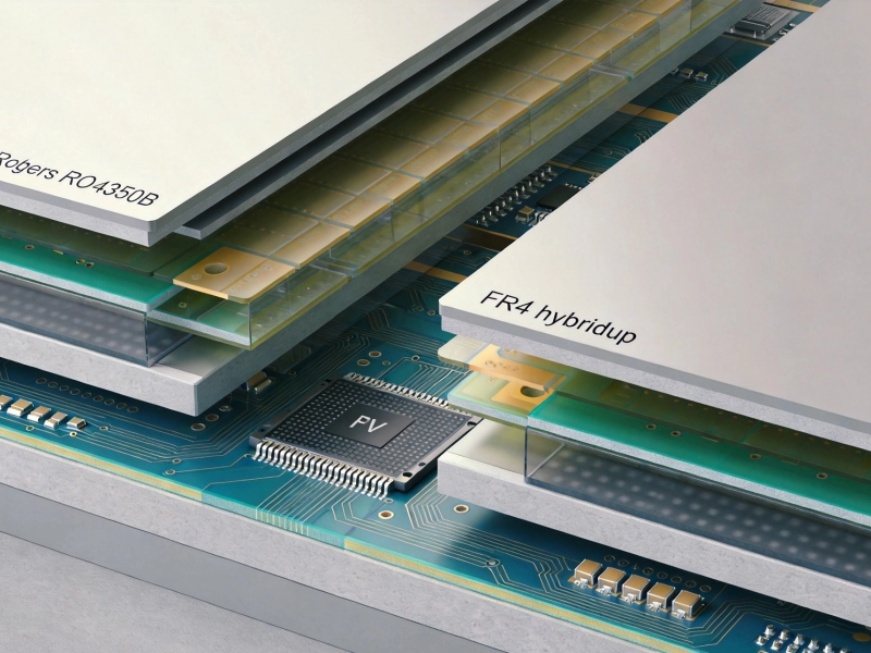
Exploring Our High Frequency PCB Capabilities in Mixed Material LaminationJuly/29/2026

High Frequency PCB Capabilities for Aerospace and Defense ApplicationsJuly/17/2026
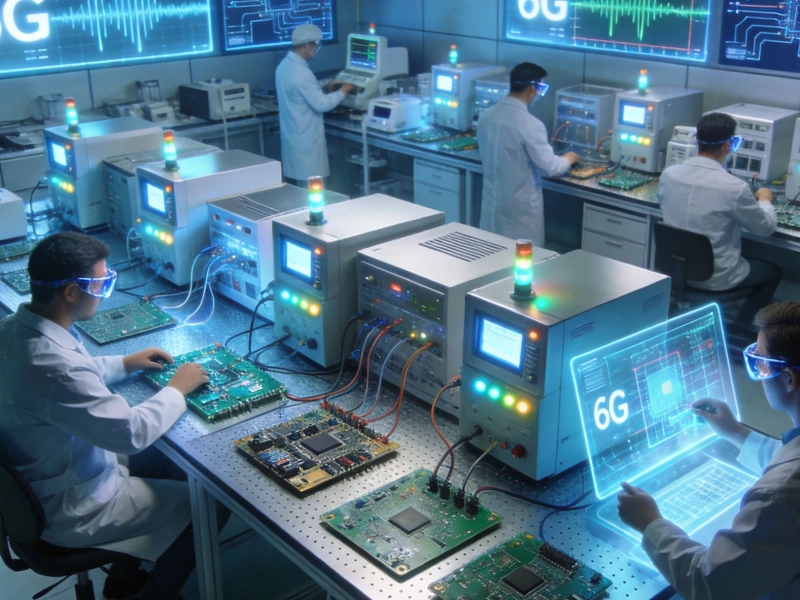
Our Latest High Frequency PCB Capabilities for 6G ResearchMay/29/2026
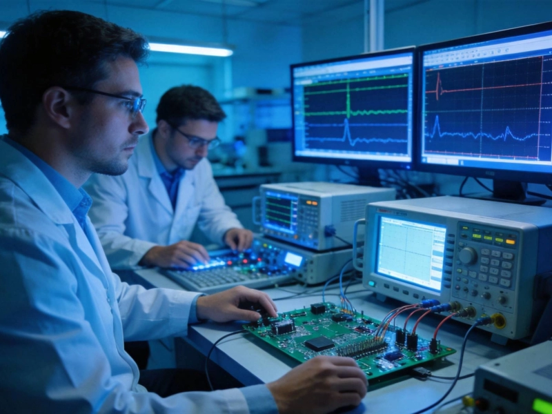
Why Advanced Testing Equipment Defines Top High Frequency PCB CapabilitiesJuly/07/2026
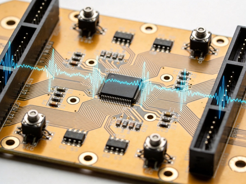
Pushing the Limits: Our Latest High Frequency PCB Capabilities for 6G ResearchJune/11/2026