Open Nav

Millimeter Wave technology—spanning the frequency range from 30 GHz to 300 GHz—is reshaping wireless communication, Automotive Radar, security imaging, and scientific instrumentation. Fifth-generation (5G) networks exploit the 28 GHz and 39 GHz bands for massive bandwidth. Automotive Radar operates at 77 GHz for long-range detection and 79 GHz for near-field imaging. Next-generation 6g Research is already probing sub-terahertz frequencies above 100 GHz. At these frequencies, the PCB is not merely a substrate that holds components—it is an integral part of the RF circuit, and its material properties and dimensional precision directly determine system performance.
Designing and fabricating PCBs for Millimeter Wave applications demands capabilities far beyond standard Fr-4 practice. This deep dive examines the material, process, and dimensional requirements that distinguish millimeter wave Pcb Manufacturing, and what it takes to deliver boards that perform reliably at frequencies where every micron and every material property matters.
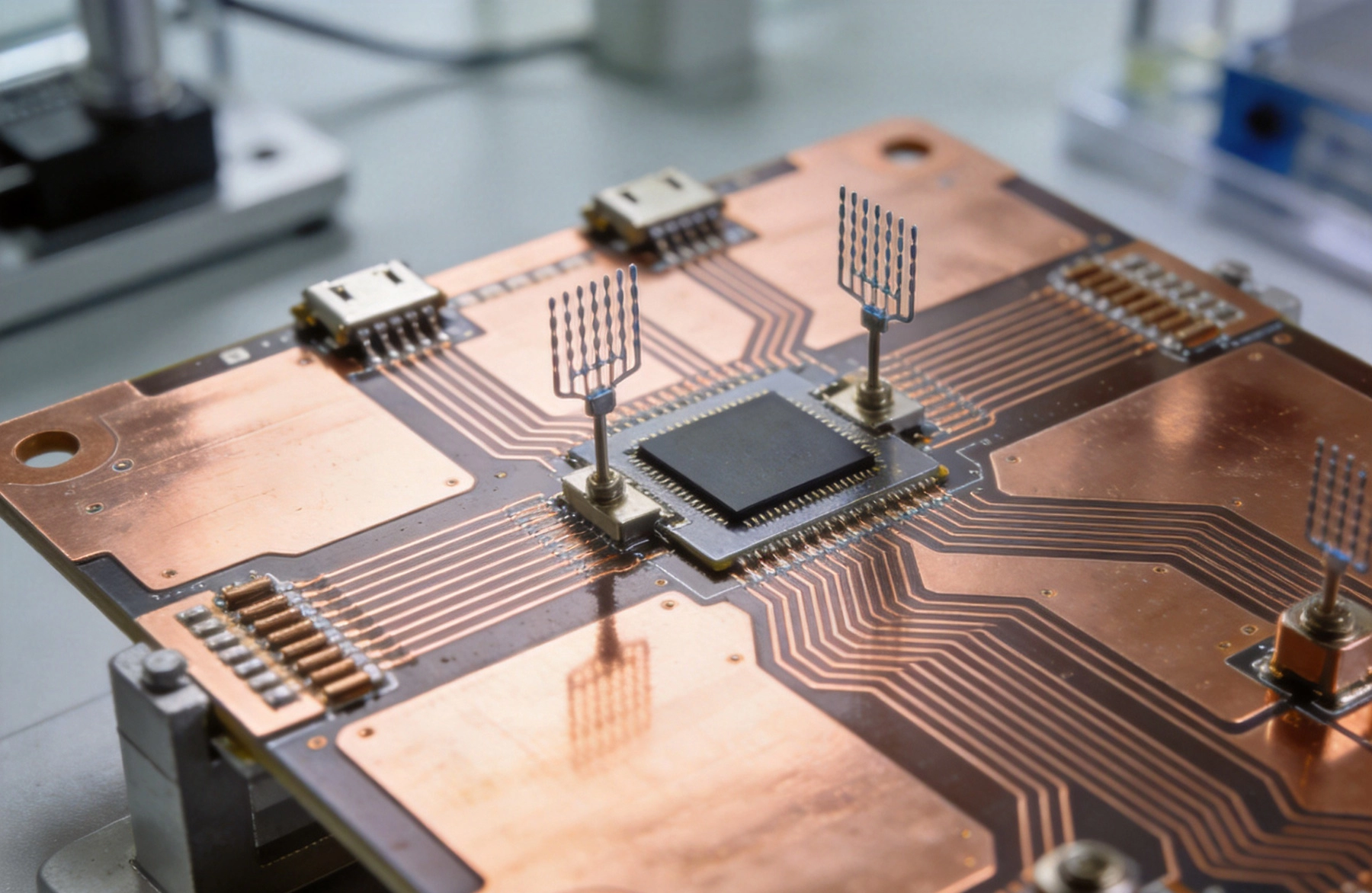
At millimeter wave frequencies, several physical effects that are negligible at lower frequencies become dominant:
At 1 GHz, a trace on standard Fr-4 (Df ≈ 0.02) might have acceptable Insertion Loss for a short run. At 77 GHz, the same material produces Insertion Loss so extreme that the signal is effectively absorbed before reaching its destination. The dielectric loss component scales linearly with both frequency and Dissipation Factor—double the frequency or double the Df, and you double the dielectric loss in dB per unit length. At millimeter wave frequencies, only ultra-Low-loss Materials (Df below 0.005, and preferably below 0.002) are viable for signal traces.
At high frequencies, current flows predominantly on the surface of the conductor (Skin Effect). The skin depth at 77 GHz in copper is approximately 0.23 µm—far thinner than a human hair. At this depth, any roughness on the copper surface becomes a significant portion of the current-carrying cross-section, effectively lengthening the current path and increasing resistance. Standard electrodeposited (ED) copper foil, with root-mean-square roughness of 1-3 µm, produces unacceptably high conductor loss at millimeter wave frequencies. Only very low-profile or Rolled Copper foils—with roughness below 0.5 µm—provide adequate performance.
At 77 GHz in a typical PTFE substrate (Dk ≈ 2.2), the wavelength is approximately 1.94 mm. A trace width variation of just 10 µm can shift the impedance by several ohms and introduce phase errors that degrade phased array antenna performance. Dimensional tolerances that are perfectly acceptable at 1 GHz become critical at millimeter wave frequencies. Trace width control, dielectric thickness uniformity, and etching precision all must be tightened significantly.
In phased array antennas—common in 5G and automotive radar—the phase relationship between array elements determines beam direction and shape. If the Dk of the substrate varies across the board (due to material inhomogeneity or manufacturing variation), the electrical length of traces varies, introducing phase errors that degrade beam quality. Dk uniformity across the panel and from panel to panel must be controlled to tolerances far tighter than standard practice.
Material choice is the single most impactful decision in Millimeter Wave Pcb design. The substrate's Dielectric Constant (Dk) and Dissipation Factor (Df) directly determine insertion loss, impedance, and wavelength—and therefore whether the board will work at all at the target frequency.
Polytetrafluoroethylene (PTFE) based laminates are the workhorse materials for millimeter wave applications. PTFE provides an inherently low Dk (around 2.1 for pure PTFE) and extremely low Df (below 0.001 for pure PTFE). Commercial PTFE-based laminates add ceramic fillers or glass fiber reinforcement to improve mechanical stability and reduce the CTE, trading some electrical performance for manufacturability.
Common PTFE-based materials and their typical properties at 10 GHz:
LCP offers a unique combination of low loss (Df ≈ 0.002-0.0045 at high frequency), excellent moisture resistance (absorption below 0.04%), and good thermal stability. Unlike PTFE, LCP is thermoplastic and can be processed using conventional lamination equipment, making it attractive for multilayer constructions. LCP's anisotropic Dk (different values in-plane vs. through-thickness) must be accounted for in design but can be leveraged for certain circuit topologies.
Most millimeter wave boards are not purely RF—there is typically digital control logic, power management, and low-frequency circuitry on the same board. A Hybrid Stackup uses Low-loss Materials (PTFE, LCP) only on the RF signal layers and standard or high-TG FR-4 on the digital and power layers. This approach significantly reduces material cost but introduces challenges:
At millimeter wave frequencies, the copper foil type is as important as the substrate material—yet it is frequently overlooked in material specifications.
Standard ED copper foil has a toothy, rough surface on the drum side (the side bonded to the laminate) with Rz roughness of 5-10 µm. This roughness creates a mechanical bond with the laminate but forces high-frequency current to follow the contours of the rough surface, significantly increasing the effective path length and therefore the conductor loss. At 77 GHz, ED copper can produce 2-3× the conductor loss of smooth copper.
Copper foil manufacturers offer low-profile (LP) and very low-profile (VLP) ED foils with controlled roughness. LP foil has Rz of 3-5 µm; VLP foil achieves Rz below 2 µm. These foils use special plating bath chemistry and deposition parameters during manufacturing to reduce the tooth structure while maintaining adequate adhesion to the laminate. VLP copper is the minimum acceptable standard for millimeter wave applications above 30 GHz.
Rolled annealed copper foil is produced by cold-rolling copper strip to the desired thickness, producing an extremely smooth surface (Rz below 1 µm, Ra below 0.2 µm). RA copper provides the lowest conductor loss at high frequency because the current flows on a nearly flat surface. However, RA copper has poor adhesion to laminates—the smooth surface provides little mechanical interlock—and is more expensive than ED copper. For PTFE laminates, a thin layer of ED copper is sometimes applied to the RA foil surface to improve adhesion (known as double-treated foil), combining the electrical benefits of RA copper with the mechanical benefits of ED copper.
For millimeter wave PCBs, always specify the copper foil type and roughness class in your fabrication drawing. Do not leave this to the fabricator's default—many fabricators default to standard ED copper unless specifically instructed otherwise. Specify VLP or RA copper for all signal layers carrying millimeter wave signals, and verify with the fabricator that the specified foil is available for the laminate you have selected.
At millimeter wave frequencies, Impedance Control tolerances must be significantly tighter than at lower frequencies to maintain acceptable return loss and insertion loss.
The impedance of a microstrip trace depends on the trace width, substrate thickness, and Dk. For a 50-ohm microstrip on RO3003 (Dk 3.0, 0.508mm substrate), the trace width is approximately 1.13mm. A ±5% impedance tolerance requires the trace width to be controlled to approximately ±0.05mm (±2 mil). This is well within standard etching capability at 1 oz copper. However, for thin substrates (0.127mm) used in compact millimeter wave modules, the trace width for 50 ohms may be only 0.28mm, and a ±5% impedance tolerance requires width control to ±0.012mm (±0.5 mil)—approaching the limit of conventional etching and requiring LDI imaging with tight process control.
The laminate manufacturer's Dk tolerance contributes to impedance variation. Standard PTFE laminates specify Dk tolerance of ±0.04 or ±0.05, which alone can cause ±1-2% impedance variation. For the tightest Impedance Control, select materials with guaranteed Dk tolerance of ±0.02 or better, and request lot-specific Dk data from the manufacturer for the production lot used on your boards.
Manufacturing millimeter wave PCBs requires process adjustments at nearly every step compared to standard FR-4 production.
At millimeter wave frequencies, the dimensional precision required for impedance control and phase matching cannot be achieved with contact printing using phototools. Phototools are subject to dimensional instability (stretch and shrink with temperature and humidity) and registration limitations. Laser direct imaging (LDI) writes the pattern directly onto the photoresist, eliminating phototool-related errors and achieving dimensional accuracy of ±5 µm or better. For millimeter wave production, LDI is not optional—it is a process requirement.
Etching must be tightly controlled to achieve the trace width precision that impedance and phase requirements demand. Key process controls include:
PTFE-based laminates require special lamination parameters:
PTFE is soft and tends to smear during drilling, coating the hole walls with insulating PTFE that blocks the copper-to-copper connection at inner layer pads. This smear must be removed by plasma desmear—a process that uses reactive ionized gas (typically oxygen or CF4/O2 mixture) to etch away the PTFE residue. Plasma desmear parameters must be optimized for PTFE: too little plasma leaves smear; too much plasma over-etches the laminate, enlarging the holes and potentially attacking the glass fiber reinforcement.
Electroless copper plating on PTFE surfaces is challenging because PTFE is chemically inert and non-wetting. The sodium etch or plasma surface treatment that improves copper-to-PTFE adhesion also affects the hole wall surface, and the electroless copper bath must be formulated to initiate reliably on the treated PTFE. Bath chemistry, activation steps, and plating parameters must be specifically qualified for PTFE substrates—standard FR-4 plating processes are not directly transferable.
Conventional PCB test methods are insufficient for verifying millimeter wave performance. Additional tests specific to high-frequency boards are required.
Insertion loss of critical RF traces must be measured using a vector network analyzer (Vna) with appropriate RF probing (coplanar or microstrip launch structures). The measured insertion loss should be compared against the simulated loss to verify that material properties and dimensional accuracy meet expectations. Discrepancies may indicate material Df variation, copper roughness deviation, or dimensional errors.
Time-domain reflectometry (Tdr) measures the impedance profile along the trace, revealing not just the average impedance but any impedance discontinuities at transitions, bends, or via locations. For millimeter wave traces, Tdr bandwidth must be high enough to resolve the short discontinuities that matter at these frequencies—a 20 GHz TDR may be insufficient for a 77 GHz application; 50 GHz or higher bandwidth is preferred.
The actual Dk and Df of the laminate in the production lot may differ from the datasheet values (which are typically measured at 10 GHz). For millimeter wave applications, verify the material properties at the operating frequency using a resonant cavity test or a microstrip ring resonator. Some laminate manufacturers provide frequency-dependent Dk and Df data up to 110 GHz; request this data for your specific material and thickness.
For phased array antenna boards, the electrical length of the feed network traces must be matched across all array elements to maintain beam quality. Phase mismatch specifications are typically ±2-5 degrees at the operating frequency. This requires both Dk uniformity across the board panel and precise trace length control—neither of which can be verified by standard Pcb Testing. Phase verification requires Vna measurement of the S-parameters of each feed path, a test that is typically performed at the module level rather than the bare board level.
A capable Millimeter Wave Pcb manufacturer does more than fabricate boards—they support your design process with data and expertise that enable first-pass success.
Request the following from your manufacturer or the material supplier:
For hybrid stackups combining low-loss and standard materials, the manufacturer should provide stackup engineering support—helping you select dielectric thicknesses that achieve target impedances while maintaining lamination compatibility and CTE balance. This is a collaborative process that requires both your circuit requirements and the manufacturer's process knowledge.
The manufacturer should be able to model the impedance of your trace structures using field-solver software that accounts for the actual copper profile (trapezoidal from etching), surface roughness correction factors, and the frequency-dependent behavior of Dk and Df. This modeling provides the trace width targets that, after etch compensation, achieve the desired impedance at the operating frequency.
5G millimeter wave base stations and user equipment require PCBs with Controlled Impedance feed networks, antenna arrays, and beamforming circuitry. The large channel bandwidths at mmWave frequencies (400 MHz to over 1 GHz) demand very low insertion loss in the feed network to preserve link budget. Typical board constructions use RO3003 or RO4003C on the RF layers with FR-4 on digital/power layers.
Automotive radar sensors operate in a harsh environment—wide temperature swings, vibration, and humidity—while demanding exceptional phase stability for accurate angle estimation. The PCB must maintain Dk stability over temperature (Dk temperature coefficient below 30 ppm/°C) and humidity (moisture absorption below 0.1%). Typical materials are RO3003 or RT/duroid 5880 with RA copper for minimum loss.
Low Earth orbit (LEO) satellite constellations for broadband internet use Ka-band (26-40 GHz) user terminals and inter-satellite links. These boards must survive the thermal cycling of orbit (typically -40°C to +85°C, thousands of cycles) while maintaining RF performance. Polyimide-based low-loss materials and heavy copper for power handling are common requirements.
Millimeter wave imaging systems for security screening operate at W-band frequencies where clothing is transparent but concealed objects are visible. These systems require PCBs with extremely low loss and precise phase control for high-resolution imaging. The small wavelengths at W-band (2.7-4.0 mm) make dimensional tolerances exceptionally critical.
Millimeter wave Pcb Manufacturing is a specialized discipline where material properties, dimensional precision, and process control converge at levels far beyond standard practice. The dielectric loss of the substrate, the surface roughness of the copper, the uniformity of the etching, and the stability of the lamination all directly affect whether the board will work at 30 GHz, 77 GHz, or 110 GHz.
Selecting the right material—PTFE-based laminate with appropriate Dk, Df, and CTE—is the foundation. Specifying low-profile or Rolled Copper foil for signal layers eliminates a major and frequently overlooked loss mechanism. Tight impedance control, verified by TDR and supported by field-solver modeling and etch compensation, maintains Signal Integrity. And specialized fabrication processes—LDI imaging, PTFE-qualified drilling and plating, controlled lamination—translate the design intent into a physical board that performs as simulated.
As millimeter wave applications proliferate—5G networks densify, automotive radar becomes standard, satellite constellations scale, and 6g Research pushes toward sub-THz frequencies—the demand for PCBs that perform reliably at these frequencies will only intensify. Engineers and manufacturers who invest in the capabilities described in this article will be positioned at the forefront of one of the most technically demanding and rapidly growing segments of the PCB industry.
Pushing the Limits: Our Latest High Frequency PCB Capabilities for 6G ResearchJune/11/2026

How Our High Frequency PCB Capabilities Support High-Speed Data CentersAugust/08/2026

Our Latest High Frequency PCB Capabilities for 6G ResearchMay/29/2026
Exploring Our High Frequency PCB Capabilities in Mixed Material LaminationJuly/29/2026
Understanding High Frequency PCB Capabilities: Line Width, Spacing, and Layer CountJune/28/2026
The Importance of Impedance Control in Our High Frequency PCB CapabilitiesSeptember/03/2026
High Frequency PCB Capabilities: Handling Thick Copper and High Power RFSeptember/15/2026

Why Advanced Testing Equipment Defines Top High Frequency PCB CapabilitiesJuly/07/2026