Open Nav

Designing a high-density RF board is one challenge. Finding a manufacturer who can produce it consistently and reliably is another. The gap between design intent and manufactured reality is wider in high-density RF work than in almost any other PCB discipline, and the consequences of a manufacturing mismatch are more severe. A board that arrives from the fabricator with impedance tolerances of plus or minus 15 percent when your design targeted plus or minus 10 percent may function adequately for consumer applications but will fall short for RF systems where Signal Integrity is measured in fractions of a decibel. Understanding what separates a capable high-density RF manufacturer from a general-purpose shop is not just procurement knowledge; it is engineering knowledge that directly affects whether your design works.
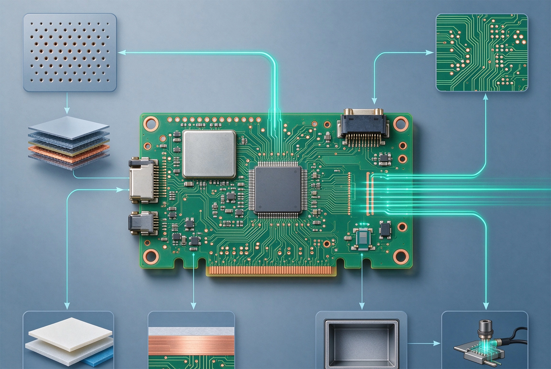
High-density RF designs combine two sets of manufacturing challenges that individually push the limits of PCB Fabrication capability. The HDI dimension demands fine features: microvias, fine lines and spaces, tight registration, and high layer counts in compact form factors. The RF dimension demands precise electrical performance: Controlled Impedance with tight tolerances, controlled dielectric properties, consistent propagation constants, and minimal Signal Loss at high frequencies. When these requirements overlap in a single board, the fabricator must excel at both, and excellence in one does not automatically guarantee excellence in the other.
The material systems used in high-density RF work compound this complexity. Standard Fr-4 is often inadequate for frequencies above a few gigahertz because its dielectric loss becomes significant and its Dielectric Constant variation with frequency is poorly controlled. Specialty materials like Rogers, Taconic, and Panasonic Megtron provide more predictable electrical properties at RF frequencies, but they have different processing characteristics than Fr-4. A manufacturer who is excellent at fine-line HDI on FR-4 may have limited experience with the same feature sizes on Rogers, which requires different lamination temperatures, different drill parameters, and different surface preparation techniques.
The measurement and verification challenge in high-density Rf Manufacturing is also distinct. Verifying that a board with 50-ohm Controlled Impedance traces actually has 50-ohm impedance requires time-domain reflectometry or vector network analysis at the relevant frequency range. This testing is not standard at most PCB shops; it requires investment in equipment, calibration, and trained personnel. A fabricator who ships high-density RF boards without impedance testing is asking you to trust their process control without measurement confirmation, which is a significant risk in precision RF work.
The foundation of high-density Rf Manufacturing is material. Not just having access to RF-grade laminates, but handling them in a way that preserves their electrical properties throughout the manufacturing process. RF-grade laminates are more sensitive to processing conditions than standard FR-4, and fabricators who do not understand these sensitivities can degrade the electrical performance of the material before the first circuit trace is even imaged.
One of the most important material handling requirements is temperature control during storage and processing. RF laminates based on Ptfe, for example, are susceptible to dimensional change if exposed to temperatures above their glass transition point during storage or prepreg bonding. The fabricator must have controlled storage conditions, appropriate handling procedures during inner layer processing, and lamination parameters that are calibrated to the specific laminate system being used. This is not complex, but it requires knowledge and discipline that not all shops have developed.
Panel preparation for RF laminates also requires specific attention. The oxide or oxide-alternative treatment used to promote adhesion between laminate layers must be controlled to avoid altering the surface roughness of the copper in ways that increase Insertion Loss at high frequencies. For some RF applications, very smooth copper is required to minimize Skin Effect losses, which means the fabricator must have alternative surface preparation processes that achieve adhesion without excessive roughening. This is a capability that requires explicit inquiry; it is not standard practice at most shops.
The ability to work with a wide range of Rf Laminate Materials is another indicator of RF manufacturing capability. A capable shop stocks or has rapid access to common Rf Materials like Rogers Ro4003c, RO4350B, RT/duroid, and Taconic Rf-35, and can provide material characterization data that confirms the electrical properties of the specific lot used in your board. They should be able to advise on laminate selection based on your frequency range, loss requirements, and thermal environment, drawing on experience across many RF applications rather than simply quoting material from a datasheet.
High-density RF designs frequently require fine lines and spaces that approach or exceed the resolution limits of standard PCB imaging processes. A board with 3-mil lines and spaces, which is common in compact RF modules, demands imaging equipment, process controls, and inspection methods that are a step beyond what is needed for standard digital boards. Not all HDI manufacturers have pushed their fine-line capability to the level required for demanding RF work.
The critical process steps for fine-line RF boards are resist application, exposure, and development. Photoresist thickness must be carefully matched to the line width requirement; too thick a resist profile can cause undercutting during development and distorted line geometries. Exposure must be precisely calibrated for the specific resist and substrate combination, and the photomask itself must have the dimensional accuracy required for the target line tolerances. For the tightest features, some manufacturers use stepper-based exposure rather than contact exposure to achieve better dimensional control.
Etch process control for fine lines requires careful management of etch time, etchant concentration, and spray pressure. Over-etching narrows lines; under-etching leaves residual conductor that narrows the spacing. For fine-line work, etch processes are often run at lower temperatures and slower rates to improve control, which increases cycle time but reduces the risk of feature distortion. The fabricator's willingness to invest this extra process time is a marker of their commitment to RF-quality work.
Inspection of fine-line features requires either automated optical inspection with sufficient resolution or, for the most demanding work, measurement with a scanning electron microscope or similar high-magnification tool. A fabricator who inspects fine-line features at standard optical magnification may miss critical defects that are only visible at higher resolution. Confirming that the manufacturer has appropriate inspection capability for the line widths in your design is an important part of vendor qualification.
Controlled impedance is the defining manufacturing capability for high-density RF work, and the quality of this capability varies dramatically between manufacturers. The difference between a fabricator who can produce plus or minus 10 percent impedance tolerance and one who can reliably achieve plus or minus 5 percent is not just a matter of equipment; it is a matter of process discipline, measurement systems, and accumulated expertise in Impedance Control across different stackups and material systems.
The basis for controlled impedance begins with accurate Dielectric Constant data for the specific material lot being used. As mentioned earlier, datasheet values for dielectric constant are nominal, and actual values vary by lot and by position within a panel. A capable RF manufacturer measures or sources measured dielectric constant data for the specific material in your production run, rather than relying on datasheet nominals. This data, combined with accurate trace geometry from the impedance calculation, provides the foundation for achieving tight impedance tolerances.
Trace geometry control, particularly the consistent蚀刻 profile and copper weight across the panel, is equally important. Impedance is a function of trace width and trace height above the reference plane, and variation in either dimension directly translates to impedance variation. For tight impedance tolerances, the fabricator must control etch profile, plating uniformity, and solder mask coverage in ways that minimize within-panel and panel-to-panel variation.
阻抗测试 is the final and most direct indicator of Manufacturing Quality. A capable RF manufacturer tests impedance on representative samples from every production panel, using Tdr or Vna methods at the frequency range relevant to your application. They provide this data as part of the delivery package, not just on request. If a manufacturer quotes controlled impedance but does not test every panel, or tests only at DC resistance rather than at RF frequencies, their claimed capability is unverified and should be treated with skepticism.
In HDI RF designs, microvias are not just routing conveniences; they are integral to the signal path and must be treated as such from an RF performance perspective. A microvia that introduces significant inductance or discontinuity in the signal path degrades the performance of an RF circuit just as surely as a poorly designed Transmission Line. Understanding how microvia design interacts with RF performance, and confirming that the manufacturer can produce microvias that meet the required RF specifications, is a critical qualification step.
The RF performance of a microvia depends on its geometry, plating quality, and the transition it creates between layers. A microvia with thick plating and a controlled entry and exit geometry has lower inductance and less reflection than one with thin or irregular plating. The aspect ratio of the microvia, the ratio of its depth to its diameter, affects the plating quality in the barrel; high-aspect-ratio microvias are more difficult to plate uniformly and may have thinner copper at the bottom of the barrel than at the entry.
Back-drilling or controlled depth drilling of through-vias is another RF-specific capability that matters for high-frequency designs. In a multilayer board carrying RF signals on internal layers, the stub created by the portion of the via extending beyond the signal layer can act as a resonant stub that degrades signal quality at certain frequencies. Back-drilling removes the stub portion of the via, but requires precise depth control to avoid damaging the signal layer connection. Manufacturers with RF experience understand when back-drilling is needed and have the equipment and process control to perform it accurately.
Via filling and capping for microvias used in RF applications requires specific attention. Filled microvias, where the barrel is filled with conductive or non-conductive material, may be used to create flat surfaces for component mounting or to improve thermal performance. For RF applications, the filling material and the via cap must not introduce discontinuities in the reference planes that affect the controlled impedance of adjacent traces. The fabricator should understand these interactions and design the fill and cap process to minimize RF impact.
A manufacturer who provides genuine stackup engineering support adds more value to a high-density Rf Design than one who simply processes the stackup as specified. Stackup engineering for RF applications requires understanding the electrical requirements of the design, the properties of the available materials, and the manufacturing process capabilities of the shop. A capable manufacturer can suggest stackup modifications that improve electrical performance, reduce cost, or improve manufacturability, drawing on experience across many similar designs.
The design review process with a capable RF manufacturer typically includes impedance verification for all controlled impedance structures, clearance and spacing review for high-voltage or high-power RF sections, thermal analysis for power dissipation, and manufacturability review for fine-line features, microvia structures, and panelization. This review should be documented and should result in a design data package that is approved by both the customer and the manufacturer's engineering team before production begins.
Dfm feedback specific to RF requirements is another differentiator. A manufacturer experienced in high-density RF work will flag design features that are problematic for RF performance even when they are manufacturable. For example, a 90-degree corner in a high-frequency trace causes reflection even though it is electrically functional; a capable RF manufacturer will recommend mitered corners and will implement them in their CAM processing if the original design did not specify them. These small improvements, accumulated across a complex design, can make a meaningful difference in RF performance.
Vendor qualification for high-density RF Pcb Manufacturing should be a structured process that verifies the specific capabilities required for your application, not just a general assessment of the manufacturer's reputation or equipment list. The qualification process should include review of the manufacturer's experience in RF-specific applications, verification of the specific material systems and stackup capabilities they are proposing to use, and evaluation of their measurement and test capabilities for the electrical parameters that are critical for your design.
Sample boards are the most direct way to verify manufacturing capability. Requesting a small number of sample boards before committing to production allows you to verify that the manufacturer can achieve the tolerances and quality level your design requires. The samples should be tested for impedance, inspected for defects, and cross-sectioned to verify layer registration, plating quality, and dielectric integrity. If the samples do not meet your requirements, the manufacturer should be willing to work with you to resolve the issues before production release.
Audit of the manufacturer's process controls, either through a formal audit program or through review of their quality documentation, provides additional confidence in their capability. The key process controls for high-density RF work include incoming material verification, process parameter monitoring and control charts, equipment calibration schedules, and final test and inspection procedures. A manufacturer who can demonstrate effective controls in these areas is more likely to deliver consistent quality over the life of a production program than one who relies on inspection to catch problems after they occur.
High-density RF Pcb Manufacturing demands a specific combination of capabilities that only a subset of PCB shops have developed. Material handling expertise for RF-grade laminates, fine-line processing control, rigorous controlled impedance capability with RF-frequency testing, microvia quality appropriate for RF signal paths, and genuine stackup engineering support are the hallmarks of a capable RF manufacturer. Finding a partner who excels in all of these areas requires due diligence that goes beyond reviewing a capability datasheet or accepting a sales representative's claims.
The investment in proper manufacturer qualification pays returns over the entire life of a product program. A well-qualified manufacturer delivers boards that meet specifications consistently, provides engineering support that improves the design over time, and responds to issues with the urgency and transparency that demanding RF work requires. A manufacturer who is chosen based on price alone, without verification of their specific RF capabilities, is a risk that frequently manifests as schedule delays, performance shortfalls, and costly redesigns. The engineering time invested in thorough vendor qualification is among the highest-return activities in high-density RF product development.
Contact us to discuss your requirements.
A Deep Dive into High Frequency PCB Capabilities for Millimeter Wave TechSeptember/24/2026

High Frequency PCB Capabilities for Aerospace and Defense ApplicationsJuly/17/2026
Understanding High Frequency PCB Capabilities: Line Width, Spacing, and Layer CountJune/28/2026

How Our High Frequency PCB Capabilities Support High-Speed Data CentersAugust/08/2026
The Importance of Impedance Control in Our High Frequency PCB CapabilitiesSeptember/03/2026
Pushing the Limits: Our Latest High Frequency PCB Capabilities for 6G ResearchJune/11/2026

Why Advanced Testing Equipment Defines Top High Frequency PCB CapabilitiesJuly/07/2026

Our Latest High Frequency PCB Capabilities for 6G ResearchMay/29/2026