Open Nav

One of the most common architecture decisions that hardware engineers face when designing a new electronic product is whether to use a standard Fr-4 PCB or a specialized High-frequency Pcb material for the system design. The wrong choice can have catastrophic consequences for both product performance and production cost: choosing a high-frequency material when a standard Fr-4 would have worked perfectly can double or triple the unit cost of the board, making the product uncompetitive in the market. Choosing standard FR-4 for a high-frequency application above 6 GHz will result in excessive Signal Loss that makes the system completely unusable, requiring a full design respin and months of schedule delay. Understanding the performance differences, the cost tradeoffs, the manufacturing complexity, and the application suitability of standard vs high-frequency PCBs is essential knowledge for any hardware engineer who wants to make optimal architecture decisions that balance performance, cost, and time-to-market.
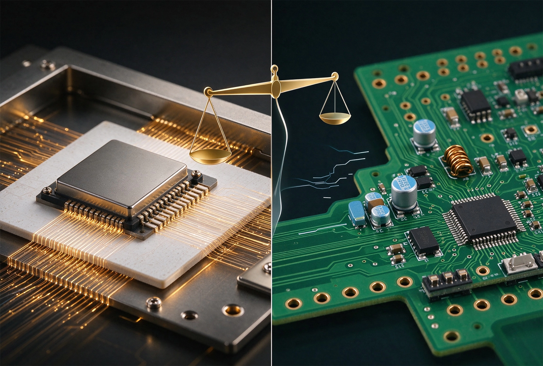
The fundamental difference between high-frequency PCBs and standard PCBs lies in the dielectric material properties that determine how electromagnetic waves propagate through the substrate material. Standard PCBs use flame-retardant 4 (FR-4) epoxy glass laminate as the base dielectric material, which is widely available, low cost, and well-understood after decades of use in the electronics industry. High-frequency PCBs use specialized Dielectric Materials engineered to have extremely stable electrical properties across wide frequency, temperature, and humidity ranges, with very low Signal Loss characteristics at microwave and Millimeter Wave frequencies.
The loss tangent (tan δ) of the dielectric material is the most important parameter that differentiates high-frequency materials from standard FR-4. Loss tangent describes the proportion of electromagnetic energy that is absorbed and dissipated as heat as the signal propagates through the dielectric. Standard FR-4 has a loss tangent of approximately 0.02 at 1 GHz, which rises to 0.03 or higher at 28 GHz. This means that roughly 3 percent of the signal energy is lost per centimeter of trace length at 28 GHz, which is completely unacceptable for any high-performance Rf Design. Specialized high-frequency ceramic-filled Ptfe materials have loss tangent values as low as 0.002 at 30 GHz, which reduces dielectric loss by more than 10 times compared to standard FR-4. Hydrocarbon ceramic laminates, the cost-optimized mid-range high-frequency material option, have loss tangent values in the 0.003 to 0.005 range at 30 GHz, striking a balance between performance and cost for commercial high-volume applications.
Dielectric Constant (Dk) stability across frequency and temperature is the second critical material property difference. Standard FR-4 has a nominal Dielectric Constant of 4.2, but this value can drift by as much as 10 percent across the operating frequency range and by 15 percent across the temperature range from -40°C to 125°C. This drift causes impedance variation that degrades Signal Integrity and creates impedance mismatches that reflect signal power back toward the source. High-frequency materials are engineered to have Dk stability within ±0.02 across the full operating frequency range up to 100 GHz, and within ±2 percent across the full industrial temperature range, ensuring consistent impedance performance and predictable signal propagation characteristics.
Moisture absorption is another important differentiator. Standard FR-4 absorbs approximately 0.2 percent of its weight in moisture when exposed to high-humidity environments, which changes the effective dielectric constant by 5 to 7 percent and increases loss tangent by 15 to 20 percent. High-frequency materials have moisture absorption rates below 0.05 percent, and premium Ptfe materials have absorption rates below 0.02 percent, which means their electrical properties remain stable even in outdoor high-humidity deployment conditions.
The material property differences between standard and high-frequency PCBs translate directly into measurable performance differences in real-world applications, especially as operating frequencies rise above 6 GHz.
Insertion Loss, the total signal power lost as it travels along a Transmission Line, is the most obvious performance difference. At 10 GHz, a 50-ohm Microstrip Transmission Line on standard FR-4 has an Insertion Loss of approximately 1.2 dB per 10 centimeters. On a high-frequency hydrocarbon ceramic laminate, the same transmission line has an insertion loss of just 0.3 dB per 10 centimeters at the same frequency. At 28 GHz 5G Millimeter Wave frequencies, the gap widens dramatically: FR-4 has insertion loss of 8 dB per 10 centimeters, while a premium PTFE high-frequency material has insertion loss of less than 1 dB per 10 centimeters. This 7 dB difference is the difference between a system that has enough link budget to communicate reliably at 300 meters versus a system that can barely communicate at 50 meters.
Impedance Control tolerance is another key performance tradeoff. Standard Pcb Manufacturing processes can achieve impedance tolerance of ±10 percent, which is more than sufficient for low-frequency digital designs and sub-6 GHz RF applications. High-frequency applications above 10 GHz require impedance tolerance of ±2 percent or better to minimize signal reflections at impedance discontinuities. Achieving this tight tolerance requires not only stable dielectric material with tightly controlled thickness, but also advanced manufacturing processes like laser direct imaging lithography that can hold trace width tolerance to within 5 microns across the full production panel. Standard FR-4 Pcb Manufacturing lines do not have this level of process control, so they cannot achieve the impedance tolerances required for high-frequency designs.
Conductor loss is significantly lower on high-frequency PCBs compared to standard PCBs, due to the use of ultra-smooth rolled-annealed copper foil instead of standard electrodeposited copper. The Skin Effect at high frequencies confines the RF current to an extremely thin layer near the copper surface, so any surface roughness on the copper dramatically increases the effective AC resistance. Standard ED copper has RMS surface roughness of 2 to 4 microns, which increases conductor loss by 2 to 3 times at 30 GHz compared to ultra-smooth rolled-annealed copper with RMS roughness below 0.3 microns that is standard on high-frequency PCBs.
Long-term reliability in extreme environmental conditions is another performance advantage of high-frequency PCBs. Standard FR-4 has a Glass Transition Temperature of approximately 130°C, above which the material softens and experiences dimensional changes that can cause solder joint fatigue and copper trace delamination. High-frequency materials have glass transition temperatures above 180°C, and premium PTFE materials have Tg above 250°C, making them suitable for high-temperature aerospace, automotive, and industrial applications that require continuous operation at elevated temperatures.
The superior performance of high-frequency PCBs comes with significant cost and lead time penalties compared to standard FR-4 PCBs, which must be carefully weighed against the performance requirements of the specific application.
Raw material cost is the largest component of the cost difference. Standard FR-4 laminate material costs approximately $0.10 to $0.20 per square centimeter for 1.6 mm thick 2-layer material. Entry-level high-frequency hydrocarbon ceramic laminate costs 3 to 5 times more than FR-4, at $0.30 to $1.00 per square centimeter. Premium PTFE ceramic-filled high-frequency materials can cost 10 to 15 times more than FR-4, at $1.00 to $3.00 per square centimeter. For complex multilayer boards with 8 or more layers, the material cost difference becomes even more pronounced, as each layer adds additional high-cost dielectric material to the stackup.
Manufacturing process complexity adds another layer of cost premium for high-frequency PCBs. Standard FR-4 PCBs are manufactured on general-purpose production lines that process thousands of panels per day, which drives down manufacturing cost through economies of scale. High-frequency PCBs require specialized manufacturing lines with advanced equipment: laser direct imaging lithography for tight trace tolerance, back-drilling equipment to remove via stubs, Controlled Impedance test equipment for every panel, and optimized lamination processes for high-frequency materials. The yield of High-frequency Pcb production is also significantly lower than standard FR-4, because any small variation in dielectric thickness, trace width, or lamination pressure can push the impedance out of tolerance. The combination of specialized equipment, lower yield, and slower process throughput makes high-frequency PCB manufacturing 3 to 12 times more expensive than standard FR-4 manufacturing for equivalent layer count and board size.
Lead time is another important tradeoff. Standard 2-layer and 4-layer FR-4 PCBs can be manufactured in 2 to 5 working days from order receipt, thanks to high-volume production lines that run 24/7. High-frequency PCBs have longer lead times of 7 to 21 working days, because the specialized materials are often not stocked in large quantities, the manufacturing process is slower, and every panel requires more detailed inspection and testing before it can be shipped. For prototype runs, the lead time difference can be even larger, as high-frequency material suppliers may have minimum order quantities that require a special order if the required material is not in stock locally.
Assembly cost for high-frequency PCBs is also 20 to 50 percent higher than standard PCBs, due to tighter Component Placement tolerance requirements, specialized reflow profile optimization, and more rigorous post-assembly Rf Testing. Fine-pitch RF components and BGA packages require placement accuracy of ±25 microns, which requires more advanced Smt placement machines than are used for standard assembly. Post-assembly testing of high-frequency boards requires specialized vector network analyzer equipment and calibrated RF test fixtures that add significant test cost per unit compared to standard in-circuit test for digital boards.
The decision to use a standard PCB or a high-frequency PCB depends entirely on the operating frequency range, performance requirements, production volume, and budget constraints of the specific application.
Standard FR-4 PCBs are the optimal choice for all applications with operating frequencies below 6 GHz, where the performance of FR-4 is more than sufficient to meet the design requirements. This includes the vast majority of consumer electronics, IoT sensors, low-speed digital boards, industrial control systems, sub-6 GHz Wi-Fi and cellular devices, and basic power supply boards. For these applications, the cost savings of using standard FR-4 far outweigh any marginal performance benefits that a high-frequency material would provide. Even many RF applications operating below 3 GHz, like Bluetooth devices, FM radios, and GPS receivers, work perfectly well on standard FR-4 with careful design and layout optimization.
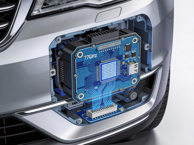
High-frequency PCBs are required for all applications with operating frequencies above 10 GHz, where the insertion loss and impedance drift of standard FR-4 would make the system unusable. This includes 5G millimeter wave systems operating in the 24 GHz, 28 GHz, and 39 GHz bands, Automotive Radar systems operating at 77 GHz and 120 GHz, satellite communication systems operating at Ka-band and V-band frequencies, Medical Imaging equipment, aerospace avionics systems, and high-speed backplane interconnects operating above 25 Gbps. For these applications, the cost premium of high-frequency materials is unavoidable, as there is no way to achieve the required performance using standard FR-4 no matter how much design optimization is done.
For applications operating in the 6 GHz to 10 GHz transition range, the choice between standard and high-frequency PCB depends on the specific performance requirements and link budget margin of the design. If the link budget has enough margin to absorb the higher insertion loss of FR-4, then standard FR-4 is a perfectly acceptable and cost-effective choice. If the link budget is tight, or if the design requires very high receiver sensitivity, then a mid-range high-frequency Hydrocarbon Laminate is likely the better choice, providing enough performance improvement to meet the requirement without the cost premium of premium PTFE materials.
For many system designs that include both high-frequency Rf Circuits and low-frequency digital circuits on the same board, a Hybrid Stackup that combines high-frequency material on the RF signal layers and standard FR-4 on the digital and power layers provides an optimal balance between performance and cost. This hybrid approach reduces the total material cost by 30 to 50 percent compared to using high-frequency material for all layers, while still providing the required RF performance on the critical signal layers.
In a typical Hybrid Stackup, the top two layers that carry the high-frequency RF signals are made from high-frequency PTFE or Hydrocarbon Laminate, while the inner layers that carry digital signals, power planes, and ground planes are made from standard FR-4. The layers are laminated together using a compatible prepreg material that provides good bond strength and stable electrical performance at the layer interface. This approach is widely used in 5G small cell radios, Automotive Radar modules, and satellite communication terminals, where it delivers the required RF performance at a significantly lower total cost than an all-high-frequency material stackup.
The hybrid stackup approach does introduce some additional manufacturing complexity, as the lamination process must be carefully optimized to bond the dissimilar materials together without delamination or dimensional distortion. The impedance at the transition between high-frequency layers and standard FR-4 layers must also be carefully simulated and optimized to avoid impedance discontinuities that would degrade signal performance. But for many system designs, these challenges are well worth the significant cost savings compared to using high-frequency material for the entire board.
The choice between high-frequency PCB and standard PCB is not a decision about which one is "better" in general, but about which one is the optimal fit for the specific performance requirements, cost target, and lead time constraints of your application. Standard FR-4 is the unbeatable choice for low-frequency, cost-sensitive applications where its mature supply chain, low cost, and short lead times provide clear advantages. High-frequency specialized materials are mandatory for applications above 10 GHz where the performance limitations of FR-4 make it completely unsuitable. For many designs operating in the transition range between 6 GHz and 10 GHz, or designs that mix high-frequency and low-frequency circuits on the same board, hybrid stackup solutions provide the ideal balance between performance and cost. The most successful hardware teams are those that understand these tradeoffs deeply and select the material that delivers exactly the required performance at the lowest possible total cost, without over-engineering or under-specifying the PCB material choice.
Contact us to discuss your high-frequency or standard PCB design requirements and to explore how our optimized material selection and manufacturing processes can help you balance performance and cost for your specific application.
SMT vs. THT: Assembly Techniques for High Frequency PCBsJuly/03/2026
High Frequency PCB Assembly for RF Modules and Antenna BoardsNovember/13/2026
Avoiding Soldering Defects in High Frequency PCB Assembly for RF ApplicationsSeptember/11/2026
High Frequency PCB Assembly Best Practices for 5G and RF ModulesJune/08/2026
Why Component Placement is Critical in High Frequency PCB AssemblyJune/25/2026
High Frequency PCB Assembly for Automotive Radar: Precision and ReliabilitySeptember/21/2026
Ensuring Signal Integrity During High Frequency PCB Assembly ProcessesJuly/15/2026
High Frequency PCB Assembly Challenges and Best PracticesOctober/29/2026