Open Nav

The transition from 4G to 5G networks represents more than an incremental improvement in wireless performance. It represents a fundamental shift in the frequencies used, the modulation schemes employed, and the architectural approaches that network operators deploy. For PCB designers and manufacturers serving the Telecommunications Infrastructure market, these changes create both significant challenges and substantial opportunities. Understanding what 5g Base Station hardware demands from PCB technology helps engineers make better design choices and helps procurement teams evaluate manufacturing capabilities with appropriate technical depth.
5G networks operate across a much wider frequency range than their predecessors. While 4G primarily used frequencies below 6 GHz, 5G extends into millimeter-wave bands above 24 GHz, with some deployments targeting frequencies as high as 86 GHz. Each frequency band presents different PCB design challenges, and the materials, constructions, and manufacturing approaches that work for sub-6 GHz may be inadequate for millimeter-wave implementations.

Pcb Materials behave differently at 5G frequencies than they do at the lower frequencies used by previous generations of wireless equipment. Understanding these behavioral differences is essential for making good material and design choices.
Dielectric loss becomes increasingly significant as frequency increases. At 28 GHz or 39 GHz, the losses in standard FR4 material are substantial enough to affect signal strength and power efficiency in ways that would be negligible at 2 GHz. This means that 5g Base Station PCBs must use low-loss Dielectric Materials throughout the RF signal paths, even if other sections of the board can use conventional materials. The additional cost of specialized materials is justified by the performance requirements of the RF section.
Dielectric Constant stability across temperature and frequency matters more at 5G frequencies. Subtle variations in Dielectric Constant cause signal velocity changes that affect Impedance Matching and phase relationships. When tolerances are tight, variations that would be insignificant at lower frequencies become sources of meaningful performance degradation. Material datasheets typically specify dielectric constant at a single frequency and temperature, so designers must understand how their chosen materials behave across the actual operating range.
Thermal expansion creates mechanical stress that is more problematic at high frequencies. PCBs expand and contract with temperature changes, and this expansion affects the precise dimensions of Transmission Lines and spacing between components. At millimeter-wave frequencies, dimensional changes of a few microns can shift performance significantly. Material selection must account for thermal expansion characteristics as well as electrical properties.
The range of Pcb Substrate Materials available for high-frequency applications has expanded significantly as 5G technology has matured. Matching material characteristics to application requirements is one of the most consequential decisions in 5g Pcb design.
Hydrocarbon ceramic laminates represent the most common choice for 5G base station Rf Circuits. Materials like Rogers Ro4003c and RO4835 offer dielectric constants around 3.4 to 3.6 with dissipation factors below 0.003, providing good Signal Integrity at frequencies up to 40 GHz and beyond. These materials process similarly to conventional laminates, making them accessible for manufacturers with standard PCB Fabrication capabilities.
Ptfe-based materials like Rogers RT/duroid series offer even lower loss characteristics for the most demanding millimeter-wave applications. Dissipation factors below 0.001 are achievable, enabling longer transmission paths with minimal attenuation. The trade-off is that Ptfe materials require more specialized processing, including specialized drilling, plating, and handling procedures. Not all PCB manufacturers can produce these materials reliably, which limits sourcing options and typically increases cost.
Hybrid constructions that combine different materials in specific board areas offer a way to balance cost and performance. The RF section of a 5G base station board might use high-performance material while Power Delivery and logic sections use less expensive conventional materials. This approach requires careful planning of layer assignments and manufacturing processes but can achieve significant cost reductions compared to all-high-performance constructions.
The way signals travel across the PCB changes fundamentally at 5G frequencies. Transmission Line design that was adequate for lower frequencies requires careful reconsideration when targeting millimeter-wave bands.
Microstrip Transmission Lines are the simplest approach for many 5G applications, but their performance depends heavily on precise control of trace width, dielectric thickness, and copper plane spacing. At 28 GHz and above, tolerances of a few microns in trace width or dielectric thickness can shift impedance enough to cause meaningful reflections. Designers must specify manufacturing tolerances that ensure Impedance Control within acceptable limits, which typically means working with manufacturers who have demonstrated capability for tight tolerance control.
Grounded Coplanar Waveguide offers advantages for some 5G applications by providing better isolation between adjacent traces and more predictable behavior across frequency. The additional ground reference around the signal trace reduces unwanted coupling and provides Shielding that becomes more important as wavelengths shrink and trace spacing decreases. Gcpw construction requires wider boards or more complex layer structures than simple Microstrip, which affects cost and routing flexibility.
Substrate integrated waveguide represents an emerging approach for the highest frequency 5G bands. SIW structures use rows of plated vias to create waveguide-like behavior within the PCB substrate, enabling lower loss transmission over longer distances than planar transmission lines can achieve. SIW design rules are more complex than conventional Transmission Line design, and manufacturing requires tight via placement accuracy, but the performance benefits at very high frequencies can justify the additional complexity.
5G base station architecture increasingly integrates antenna elements directly with RF circuitry, creating PCB design challenges that extend beyond conventional board layout. The boundary between antenna, feed network, and RF circuitry blurs in ways that require holistic design approaches.
Phased array antennas used in massive MIMO base stations contain hundreds of antenna elements, each connected to a dedicated RF chain. The PCBs that form these antenna modules must route signals from hundreds of element positions to IC package locations with minimal loss and phase consistency. Consistency is critical because phase errors between antenna elements distort beamforming performance. Any systematic variation between signal paths translates directly into beamforming errors that reduce network coverage and throughput.
IC packaging for 5G RF applications uses advanced package types like embedded wafer-level ball grid arrays and fan-out wafer-level packaging to achieve the miniaturization and performance required. These packages have their own substrate requirements that interact with the PCB design. The transition from IC package to PCB must be designed carefully to maintain Signal Integrity, which often means co-designing the IC package and the PCB together rather than treating them as separate problems.
Thermal Management in integrated antenna modules requires solving heat flow through materials that may include high-dielectric ceramics, organic laminates, metal heat spreaders, and adhesive layers. Each material interface introduces thermal resistance, and the heat generated by power amplifiers and RF transceivers must be conducted away efficiently to maintain reliable operation. Material selection for antenna modules must account for both electrical and thermal performance simultaneously.
The performance requirements of 5G base station PCBs impose manufacturing constraints that go beyond typical production capabilities. Evaluating manufacturer capability requires understanding what matters for millimeter-wave performance.
Trace width and spacing tolerances directly affect Impedance Control and signal routing consistency. At millimeter-wave frequencies, the impact of dimensional variation is amplified, which means manufacturing processes must be held to tighter tolerances than conventional boards require. Manufacturers with statistical process control systems and demonstrated capability for tight dimension control are better choices for 5G applications.
Plating quality affects Insertion Loss and reliability. The Skin Effect at high frequencies concentrates current near conductor surfaces, which means surface smoothness and plating uniformity matter more than they do at lower frequencies. Uneven plating or rough surfaces increase effective resistance and cause additional loss. Some manufacturers specify plating thickness and surface finish requirements for high-frequency applications that exceed their standard production specifications.
Registration accuracy between layers and across the board affects yield in complex multilayer 5G constructions. Misregistration between layers can cause impedance discontinuities at via transitions or break Ground Plane continuity in ways that affect electromagnetic performance. Board manufacturers with advanced imaging and lamination controls can achieve better layer-to-layer registration than those using older equipment.
Validating 5g Pcb performance requires measurement approaches that are more sophisticated than those used for lower-frequency circuits. The cost of test equipment and the expertise required to interpret results both increase substantially.
Vector network analysis provides the fundamental measurement capability for RF performance validation. Vna measurements of S-parameters reveal how the PCB transmits and reflects signals at each frequency of interest. A quality Vna capable of measurements to 50 GHz or beyond represents a significant capital investment, and not all manufacturers or designers have access to this equipment. Working with partners who have appropriate test capability is essential for validating 5G PCB designs.
Time domain reflectometry complements frequency domain measurements by revealing the location of impedance discontinuities along signal paths. Tdr can identify problems like unexpected stubs, inadequate ground reference, or plating variations that degrade high-frequency performance. This diagnostic capability helps identify root causes when frequency domain measurements show elevated loss or poor matching.
Environmental testing validates that performance is maintained across the temperature range and lifetime expectancies required for base station operation. Outdoor base station equipment faces extreme temperatures, humidity, and thermal cycling, and PCBs must maintain performance through these conditions. Accelerated life testing and thermal cycling validation are essential for telecom infrastructure products where replacement costs are high and reliability expectations are measured in decades.
The 5G infrastructure buildout has driven significant investment in high-frequency Pcb Manufacturing capability, but supply chain dynamics remain complex. Understanding the current landscape helps with sourcing decisions and long-term supply planning.
High-frequency laminate availability has improved as material suppliers have expanded production to meet 5G demand, but lead times can still be extended for specialized materials with unique specifications. Designers who specify readily available materials from established product lines face shorter lead times than those requesting custom specifications or less common material grades. Building relationships with laminate distributors who maintain inventory helps smooth supply variability.
Manufacturing concentration in Asia remains significant for high-frequency PCBs because the specialized equipment and process expertise required is concentrated there. The logistics and geopolitical considerations that affect supply chain risk for conventional electronics also apply to 5G PCBs, but the specialized nature of millimeter-wave manufacturing limits the diversification options available. Some customers are working with Asian manufacturers to establish inventory buffers that provide supply continuity even if logistics disruptions occur.
Technology evolution continues to push toward higher frequencies, wider bandwidths, and more integrated architectures. The next generation of wireless technology already being researched will push further into the millimeter-wave spectrum and demand even more sophisticated PCB solutions. Manufacturers who invest in capability development now will be positioned to serve these future requirements as they transition from research to deployment.
5G base station hardware demands PCB technology that is more sophisticated than anything required for previous wireless generations. The combination of millimeter-wave frequencies, massive MIMO antenna architectures, and demanding reliability requirements creates design and manufacturing challenges that test the limits of current technology.
Successful 5G PCB development requires careful attention to material selection, transmission line design, manufacturing capability, and test validation. The cost and complexity of getting these elements right is significant, but the performance requirements of 5G networks do not allow shortcuts. Engineers and procurement teams who understand these requirements are better positioned to make good decisions about design approaches, manufacturing partners, and quality verification strategies.
As 5G networks continue their global rollout and as research begins targeting future wireless generations, the demand for High-frequency Pcb expertise will continue to grow. Building relationships with capable manufacturing partners now creates the foundation for successful product development over the coming years.
Contact us to discuss your requirements and explore how High-frequency Pcb capabilities can support your 5G base station hardware development.
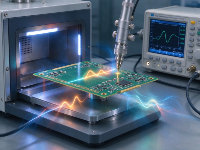
How to Test and Verify the Quality of High Frequency PCB MaterialsOctober/14/2026

Exploring High Frequency PCB Applications in High-Speed Data CentersSeptember/30/2026

High Frequency PCB Materials for Automotive Radar: Durability and SpeedSeptember/26/2026

High Frequency PCB Knowledge: The Difference Between High-Speed and High-FrequencySeptember/17/2026
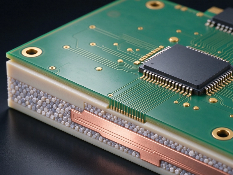
Rogers, PTFE, and Ceramic Filled Materials for High Frequency PCB FabricationOctober/23/2026
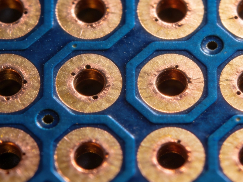
Laser Drilling and Microvias in Modern High Frequency PCB FabricationJuly/07/2026
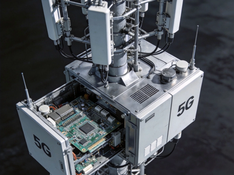
Top High Frequency PCB Applications in the 5G and Telecommunications IndustryMay/29/2026
High Frequency PCB Capabilities: Handling Thick Copper and High Power RFSeptember/15/2026