Open Nav

Requesting a quote for a High-frequency Pcb is fundamentally different from requesting a quote for a standard digital board. On a digital board, the primary specifications that determine manufacturability are the layer count, the copper weight, the minimum trace width and spacing, and the surface finish. If those parameters are within the fabricator's capability, the board can be built. On a high-frequency board, those same parameters matter, but a much larger set of specifications determines whether the board will meet its RF performance requirements: the Dielectric Constant and its tolerance, the Dissipation Factor, the dielectric homogeneity, the Impedance Control accuracy, the Copper Surface Roughness, and the dimensional stability of the substrate. A fabricator who can produce the board mechanically may not be able to produce it electrically, and the difference between a board that looks right and a board that performs right can be subtle and expensive to discover after delivery. The quotation process is your opportunity to verify that the fabricator can meet all of the requirements, not just the mechanical ones, before you commit your design and your budget to a production run. Asking the right questions before quoting, and evaluating the answers critically, separates successful high-frequency sourcing from costly learning experiences.

The substrate material is the foundation of High-frequency Pcb performance, and the first set of questions should establish whether the fabricator can procure and process the specific material your design requires.
What specific Rf Materials do you stock or procure regularly? This question distinguishes fabricators who work with Rf Materials as a routine part of their business from those who will order a specialty material as a one-time custom request. A fabricator who stocks Rogers Ro4003c, RT/duroid 5880, or other common RF materials has the purchasing relationships, the incoming inspection procedures, and the process recipes needed to produce reliable boards on those substrates. A fabricator who does not stock any RF materials will need to order the material specifically for your job, adding lead time and the risk that they may not have experience processing it.
What is your experience level with the specific material I am specifying? Experience matters because RF materials process differently than standard Fr-4 in ways that affect yield and reliability. Ptfe-based materials require special drilling parameters to prevent resin smear in the via barrels, different plasma desmear chemistry, and careful lamination control to prevent delamination. Ceramic-filled hydrocarbon materials have different etching characteristics and may require adjusted etch compensation factors. A fabricator who has produced hundreds of panels on the specific material you need can provide process data, yield information, and design-for-manufacturing guidance that an inexperienced fabricator cannot. Ask for references or for examples of similar boards they have produced on the same material.
Can you support mixed-dielectric stack-ups? Many high-frequency designs combine a low-loss RF substrate for the Microwave Circuits with standard Fr-4 for the digital control and power circuits on the same board. These mixed stack-ups require lamination processes that can bond dissimilar materials reliably, managing the different thermal expansion coefficients, lamination temperatures, and adhesion characteristics of the different laminates. A fabricator who has never produced a mixed-dielectric board may experience delamination, registration errors, or dimensional instability that are not encountered on single-material boards. If your design uses a mixed stack-up, verify that the fabricator has experience with the specific material combination you are using.
What is the available dielectric thickness for the material I need? The dielectric thickness between the signal layer and the reference plane determines the trace width needed to achieve the target impedance, and not all thicknesses are available in all materials. RF laminates are typically available in a range of standard thicknesses, but the specific thickness required by your impedance calculation may not be a standard product. If the required thickness is not available, the designer must adjust the trace width or the stack-up to accommodate a standard thickness, or the fabricator must stack multiple prepreg sheets to achieve the non-standard thickness, which may affect the Dielectric Constant and the loss tangent of the resulting composite. Confirming the available thicknesses before finalizing the stack-up prevents the need for redesign after the quotation.
The dielectric constant of the substrate directly determines the impedance, the propagation velocity, and the wavelength of signals on the board. The tolerance on the dielectric constant determines how tightly those parameters can be controlled, which affects whether the RF circuit will meet its performance specification. These questions probe the fabricator's ability to deliver boards with the Dk accuracy your design requires.
What Dk value should I use for simulation, and how does it relate to your process? The Dk value in the material datasheet is measured under specific test conditions that may not match the conditions in your actual board. The effective Dk of the manufactured board depends on the frequency, the trace geometry, the copper distribution, and the resin content in the specific area of the board. An experienced fabricator can tell you the Dk value they have verified through Impedance Measurement of test coupons, which may differ slightly from the nominal datasheet value. Using the fabricator's verified Dk value for simulation produces impedance calculations that match the manufactured board more closely than using the datasheet nominal.
What is the Dk tolerance you can guarantee for the specified material? The Dk tolerance includes the lot-to-lot variation in the material manufacturing, the within-panel variation caused by resin content distribution and glass weave effects, and the measurement uncertainty of the verification method. Standard RF materials are typically specified with Dk tolerances of plus or minus 0.04 or tighter, but the actual variation that the fabricator observes in their production may be larger or smaller than the datasheet specification depending on their process control and their relationship with the material supplier. A fabricator who provides a realistic Dk tolerance based on their production experience, rather than just quoting the datasheet specification, gives you a more reliable basis for your impedance and wavelength tolerance analysis.
How do you verify the Dk of the material you receive? Incoming material verification methods range from none, where the fabricator accepts the supplier's certificate of conformance without independent testing, to full electrical characterization using resonant cavity or stripline test methods. The rigor of the incoming verification affects the probability that an out-of-specification material lot is detected before it is used in production. For high-frequency applications where the Dk tolerance is critical, a fabricator who performs incoming Dk verification provides an additional quality gate that reduces the risk of boards with incorrect dielectric properties reaching the customer.
What is the frequency dependence of Dk for the material in my application, and can you characterize it? Most RF materials exhibit some variation of Dk with frequency, and this variation can cause the circuit behavior at the operating frequency to differ from the behavior predicted at the simulation frequency. A fabricator who can provide Dk data at frequencies relevant to your application, either from their own measurements or from detailed material characterization data, enables more accurate simulation and reduces the risk of performance discrepancy between simulation and measurement. If the fabricator cannot provide frequency-dependent Dk data, you will need to obtain it from the material manufacturer or from published literature and account for it in your design tolerance analysis.
Controlled Impedance is the specification that most directly connects the PCB Fabrication process to the RF circuit performance, and the Impedance Control capability of the fabricator determines whether your Transmission Lines will meet their impedance targets in the delivered boards.
What impedance tolerance can you achieve for the specified stack-up and trace geometry? The impedance tolerance depends on the fabricator's control of the trace width, the trace thickness, the dielectric thickness, and the dielectric constant, all of which contribute to the impedance calculation. A fabricator who claims plus or minus 10% impedance tolerance on a stack-up with tight dielectric spacing and narrow traces may be quoting a generic capability that their actual process cannot achieve for your specific geometry. Ask for impedance yield data or process capability indices for boards similar to yours that they have produced on the same material and stack-up. A Cpk of 1.33 or higher for impedance indicates a capable process; a Cpk below 1.0 indicates a process that cannot consistently meet the specified tolerance.
Do you include impedance test coupons on the production panel, and what test method do you use? Impedance test coupons are dedicated test structures, typically a set of representative Transmission Lines, that are fabricated on the same panel as the production boards and measured using time-domain reflectometry to verify the impedance of the panel before the boards are shipped. Without test coupons, there is no direct measurement of the impedance of the delivered boards; the customer must trust that the process produced the correct impedance based on the process control parameters. For high-frequency applications where impedance accuracy is critical, test coupons on every production panel provide the verification needed to confirm that the specified impedance is achieved. The test method should be specified; time-domain reflectometry with appropriate reference planes and de-embedding is the standard method for measuring PCB trace impedance.
How do you adjust for etch factor when calculating impedance-controlled trace widths? The etching process produces traces that are narrower than the artwork width due to lateral etching of the copper, and the etch factor, the ratio of lateral etch to vertical etch, varies with the copper thickness, the etching chemistry, and the copper distribution on the panel. A fabricator who accounts for etch factor by applying a width compensation to the artwork produces traces that match the specified width after etching, achieving the target impedance. A fabricator who does not compensate for etch factor produces traces that are narrower than specified, with impedance that is higher than the target. The etch compensation method and the typical compensation values for the specified material and copper weight should be discussed during the quotation process.
What is your process for adjusting impedance if the measured value is out of specification? Even with good process control, some panels may produce impedance that is outside the specified tolerance. The corrective action process should include root cause analysis to determine whether the deviation is due to trace width, dielectric thickness, or dielectric constant variation, and corrective action to bring the process back into control. For boards that are already fabricated with out-of-spec impedance, the disposition should be clearly defined: are the boards scrapped, or are they shipped with a deviation report that the customer must accept? The disposition policy should be agreed upon before the production order is placed.
Beyond material and impedance, the general manufacturing process capabilities of the fabricator determine whether the board can be produced reliably at the required quality level. These questions address the process capabilities that are most relevant to high-frequency boards.
What is your minimum finished trace width and spacing for the specified copper weight and material? The minimum trace width and spacing that the fabricator can produce reliably depends on the copper weight, the etching process, and the substrate material. Heavy copper weights are more difficult to etch with fine resolution because the longer etching time increases lateral etching, narrowing the traces and widening the spaces. RF materials with different resin systems may etch differently than standard FR-4. A fabricator who claims 4mil trace and space capability on 1oz FR-4 may not achieve the same capability on 2oz copper on a ceramic-filled substrate. Verify the specific capability for your material and copper weight combination, not just the general capability claim.
What via types do you support, and what are the minimum via dimensions for each type? High-frequency boards may use standard through-hole vias, blind vias, buried vias, or microvias depending on the routing density and the frequency requirements. Each via type has different minimum dimensions, different aspect ratio limits, and different reliability implications that must be compatible with the design. Verify that the fabricator can produce the via types and dimensions specified in the design, and ask about the reliability data for high-aspect-ratio vias in the specified material. Vias in Ptfe materials are more susceptible to plating defects than vias in FR-4 because the PTFE substrate has different adhesion characteristics and requires different plating process parameters.
What surface finishes do you offer, and what is the impact of each on high-frequency performance? The surface finish affects the conductor loss at high frequencies because the finish material has different conductivity and different surface roughness than bare copper. HASL finish produces an uneven surface with high roughness that increases conductor loss at microwave frequencies. ENIG finish provides a smooth nickel-gold surface with lower loss than HASL, but the nickel layer has higher resistivity than copper, which increases the conductor loss compared to bare copper. Immersion silver and immersion tin provide thin, smooth coatings with lower impact on conductor loss than ENIG. Bare copper with organic solderability preservative provides the lowest conductor loss but has limited shelf life and solderability. The fabricator should be able to recommend the surface finish that provides the best balance of RF performance, solderability, and cost for your specific application.
What is the Copper Surface Roughness you achieve, and how does it affect conductor loss at my operating frequency? Copper surface roughness contributes to conductor loss at frequencies above approximately 5 GHz because the skin depth of the current becomes comparable to the roughness feature size, causing the current to follow a longer path along the rough copper surface. Standard electrodeposited copper has a roughness of 2 to 5 microns RMS, which increases conductor loss by 20 to 50 percent compared to smooth copper at 10 GHz. Low-profile and very-low-profile copper foils with roughness below 1 micron are available for high-frequency applications but may have lower peel strength that affects reliability. A fabricator who understands the copper roughness impact on conductor loss can recommend the appropriate copper type for your frequency range and can provide roughness data for the specific copper foil they use.
The testing and Quality Assurance processes for high-frequency boards must verify the RF performance parameters that determine whether the board will function as designed, not just the structural parameters like continuity and isolation that are tested on digital boards.
What electrical testing do you perform on high-frequency boards, beyond standard continuity and isolation? Standard electrical testing verifies that every net is continuous and that there are no shorts between adjacent nets, but it does not verify the RF performance parameters like impedance, Insertion Loss, or return loss. A fabricator who offers RF-specific testing can verify that the board meets its RF specifications before shipment, providing a quality gate that catches RF performance problems that standard electrical testing would miss. The specific tests available should be discussed, including whether the fabricator can perform Insertion Loss measurements, return loss measurements, or Tdr impedance profiling on production boards.
What is your first-pass yield for boards similar to mine on the specified material? The first-pass yield, the percentage of boards that pass all inspections without rework on the first attempt, is a direct indicator of the fabricator's process capability for the specific board type. A low first-pass yield indicates that the process is being pushed near or beyond its capability limit, which means that some boards that pass inspection may have marginal quality that could cause field failures. A high first-pass yield indicates a comfortable process margin that produces consistent quality. Ask for yield data on boards of similar complexity, layer count, and material to yours, not just the overall factory yield which may be dominated by simple boards.
What inspection criteria do you apply to high-frequency boards? The inspection criteria for high-frequency boards should include the standard IPC-A-600 acceptance criteria plus additional criteria that are specific to RF performance. These additional criteria may include maximum conductor width reduction from etching, which affects impedance; minimum plating thickness in via barrels, which affects via reliability and current carrying capacity; and maximum surface roughness, which affects conductor loss. A fabricator who applies only standard IPC criteria to high-frequency boards may ship boards that meet the visual and dimensional acceptance criteria but do not meet the RF performance requirements.
How do you handle non-conforming boards discovered during production? The disposition of non-conforming boards, whether they are scrapped, reworked, or shipped with a deviation report, affects the quality of the delivered product. For high-frequency boards, rework is often not possible because the rework process, like re-etching to adjust trace width, may change the RF performance in ways that are difficult to predict or verify. A fabricator who scraps non-conforming high-frequency boards rather than attempting rework provides higher confidence in the delivered quality, at the cost of a potentially higher price to cover the scrap rate. The non-conforming disposition policy should be discussed and agreed upon during the quotation process.
The lead time for high-frequency boards is typically longer than for standard FR-4 boards because the materials may not be in stock, the processing times are longer for some steps like PTFE drilling and plating, and the quality verification is more extensive. Understanding the lead time drivers and the fabricator's capacity to meet your schedule is essential for planning the development and production timeline.
What is your standard lead time for the specified material and complexity, and what drives the lead time? The lead time should be broken down into its components: material procurement, fabrication, and testing. If the material procurement is the lead time driver, the lead time can potentially be reduced by providing the material on consignment or by the fabricator stocking the material against future orders. If the fabrication time is the driver, the lead time can potentially be reduced by expedited processing or overtime manufacturing. Understanding which component drives the lead time enables targeted actions to compress it.
Can you provide a quick-turn option, and what is the premium and the risk? Quick-turn fabrication of high-frequency boards accelerates the process by priority scheduling, overtime manufacturing, and compressed inspection, but it may increase the risk of quality problems because some process steps are rushed or some inspections are abbreviated. The quick-turn premium and the specific quality risks should be discussed explicitly. For prototype builds where the boards will be thoroughly bench-tested, the quality risk may be acceptable. For production builds where the boards will be shipped directly to the customer, the same quality risk may not be acceptable.
What is your current capacity utilization, and how will you prioritize my order if capacity is constrained? Capacity utilization above 85 percent typically indicates a factory that is running near its limit, with limited ability to absorb schedule acceleration or demand increases. A fabricator who is running at high utilization may prioritize large-volume customers over small-volume customers during periods of peak demand, potentially extending the delivery date for smaller orders. Understanding the capacity situation and the priority policy helps set realistic delivery expectations and identify the risk of schedule delays during peak periods.
High-frequency boards for demanding applications may require documentation and traceability that goes beyond what is standard for commercial PCB Fabrication. Verifying the fabricator's documentation capability during the quotation process ensures that they can provide the records you need without discovering after delivery that the documentation is incomplete or unavailable.
What documentation do you provide with the finished boards? The standard documentation package typically includes the fabrication data, the inspection report, and the shipping documents. For high-frequency boards, additional documentation may include impedance test reports with Tdr profiles, material certificates of conformance with Dk and Df data, first article inspection reports with microsection photographs, and dimensional measurement reports. The specific documentation requirements should be specified in the purchase order, and the fabricator should confirm that they can provide all requested documents.
Can you provide material lot traceability from the finished board back to the raw material? Traceability from the finished board to the raw material lot is important for field failure investigation and for regulatory compliance in some applications. The traceability system should allow the customer, given a board serial number or a delivery lot number, to identify the specific lots of laminate, prepreg, and copper foil that were used to produce that board. This traceability enables targeted investigation if a material quality problem is discovered after boards have been shipped, allowing only the boards produced from the affected material lot to be recalled rather than the entire production quantity.
Do you provide a certificate of conformance that includes the specific RF parameters? A certificate of conformance that attests only to general compliance with the purchase order is less valuable than one that includes the specific measured values of the RF parameters that matter most, like the measured impedance, the measured dielectric thickness, and the measured plating thickness. A fabricator who provides a detailed certificate of conformance with specific measured values demonstrates the measurement capability and the quality system rigor that support reliable RF board production.
Understanding the cost structure of the quotation enables informed cost management decisions and prevents surprises when the final invoice arrives. These questions probe the cost components and the pricing structure of the fabricator's quotation.
Can you provide an itemized cost breakdown? An itemized breakdown that separates the material cost, the fabrication cost, the impedance testing cost, and any premium for quick-turn or small-quantity processing reveals where the cost is concentrated and where leverage exists for cost reduction. A single lump-sum unit price provides no insight into the cost structure and prevents targeted cost optimization. If the fabricator is willing to provide an itemized breakdown, it also demonstrates transparency and a willingness to collaborate on cost management.
What is the NRE or tooling cost for this design, and is it one-time or recurring? Some fabricators charge NRE fees for the engineering time required to review the design, create the manufacturing instructions, and set up the impedance test coupons. These fees are typically one-time charges for the first production run and may be waived for subsequent runs. Other fabricators include the NRE cost in the unit price, which means it is amortized across the order quantity and is effectively charged again on each reorder. Understanding the NRE structure affects the total cost comparison between fabricators and the cost of reordering.
What is the price structure for reorders, and are there volume price breaks? The reorder price structure determines the cost of the product over its production lifetime, not just the first order. A fabricator who offers a lower unit price on reorders because the NRE has already been recovered provides a different lifetime cost than a fabricator who charges the same unit price on every order. Volume price breaks, where the unit price decreases at specific quantity thresholds, provide incentive for larger orders but may not be economical if the demand does not justify the larger quantity. The price structure for reorders and volume breaks should be discussed during the quotation process so that the lifetime cost can be estimated and compared between suppliers.
Are there any cost surcharges I should be aware of, such as small-lot fees, impedance test fees, or material minimum order quantities? Cost surcharges that are not included in the quoted unit price can significantly inflate the actual cost of the order. Small-lot fees are charged on orders below the fabricator's minimum economic batch size. Impedance test fees cover the cost of the test coupons and the TDR measurement. Material minimum order quantities may require the purchase of more laminate material than is needed for the order, with the excess material cost passed to the customer. Identifying all potential surcharges during the quotation process prevents unexpected charges on the invoice.
The most reliable indicator of a fabricator's ability to produce your high-frequency board is their track record with similar boards for other customers. While confidentiality restrictions may limit the specific information a fabricator can share, they can often provide general descriptions of similar work they have done.
Can you provide references or examples of similar high-frequency boards you have produced? Similar means the same material, the same layer count, the same impedance requirements, and the same general application frequency range. A fabricator who has produced boards with the same Rf Material, the same Controlled Impedance specifications, and the same copper weight as your design has demonstrated the specific capability you need. A fabricator who has produced RF boards in general but not on your specific material may be capable but represents a higher risk because they will be learning the material's process requirements on your project.
What is the longest-running RF product you currently support in production? This question assesses the fabricator's ability to sustain production of an RF board over the product lifecycle, not just to produce a one-time prototype. A fabricator who has been producing the same RF board for five years or more has demonstrated that they can maintain process control, manage material availability, and sustain quality over time. This long-term production experience is particularly important for industrial and aerospace applications where the product lifecycle extends for many years and the fabricator must remain capable and committed throughout.
Have you experienced any significant quality issues with high-frequency boards, and how were they resolved? This question probes the fabricator's problem-solving capability and their transparency about quality issues. Every fabricator experiences quality problems; the differentiator is how they respond to them. A fabricator who describes a past problem, the root cause they identified, the corrective action they implemented, and the effectiveness verification they performed demonstrates the quality system maturity that supports reliable production. A fabricator who claims they have never had a quality problem is either exceptionally lucky or not being forthcoming.
The quotation process for high-frequency Pcb Fabrication is an information-gathering exercise that determines whether the fabricator can meet the full set of requirements, not just the mechanical ones. The questions described in this article, covering material capability, Dk tolerance, impedance control, process capability, testing, lead time, documentation, cost structure, and track record, provide a comprehensive framework for evaluating a fabricator's high-frequency capability before committing to a production order.
The time invested in asking these questions before quoting pays back through better supplier selection, more accurate cost and schedule expectations, and fewer surprises during production. A fabricator who answers these questions thoroughly and transparently is demonstrating the technical competence and the business integrity that support a productive long-term manufacturing relationship. A fabricator who cannot or will not answer specific questions about their process capability may be a higher-risk choice for high-frequency manufacturing, regardless of how attractive their unit price may be. The right high-frequency PCB fabricator is the one who can produce your board reliably and measurably, not just the one who quotes the lowest price.
Contact us to discuss your high-frequency PCB requirements and receive a detailed quotation that addresses all of your technical and quality specifications.

How to Evaluate a High Frequency PCB ManufacturerOctober/26/2026

How to Vet a High Frequency PCB Manufacturer for 5G and Millimeter Wave ProjectsJuly/25/2026
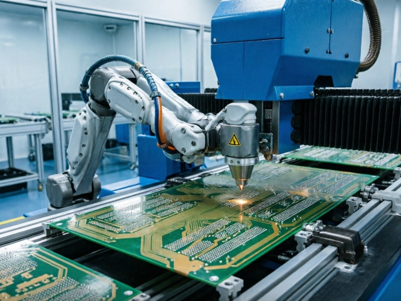
From Prototype to Mass Production: Scaling with a Reliable High Frequency PCB ManufacturerJuly/13/2026
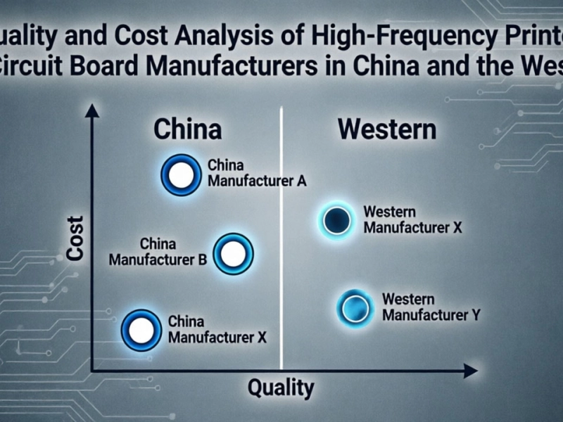
Quality and Cost Analysis of High-Frequency Printed Circuit Board Manufacturers in China and the WestJune/04/2026

Why Certifications Matter: IATF16949 and ISO Standards for Your High Frequency PCB ManufacturerJune/17/2026
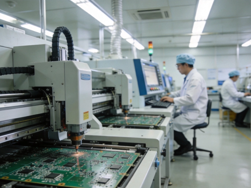
Top 5 Questions to Ask Your High Frequency PCB Manufacturer Before Placing an OrderAugust/14/2026
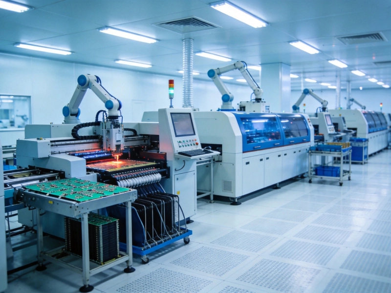
Inside the Factory: What to Look for in a High Frequency PCB Manufacturer's FacilityAugust/03/2026

How High Frequency PCB Applications are Powering the AI Server RevolutionAugust/03/2026