Open Nav

high frequency PCB projects sit at the intersection of two demanding manufacturing disciplines, each of which pushes the fabrication capabilities of a Pcb Manufacturer in different directions. High frequency applications, used in telecommunications, radar, aerospace, and advanced automotive systems, require specific substrate materials with controlled dielectric properties and tight impedance tolerances. HDI technology, which uses microvias and fine-line circuitry to achieve high interconnection density in a compact form factor, requires Precision Manufacturing processes that are several generations beyond standard PCB Fabrication. A project that combines both high frequency and HDI requirements is among the most challenging in the PCB industry, and not all manufacturers have the capability, the equipment, or the experience to support it reliably. Understanding how an HDI manufacturer with high frequency expertise approaches these projects, and what specific capabilities are required to deliver a successful outcome, helps engineers and procurement professionals select the right manufacturing partner and communicate their requirements effectively.
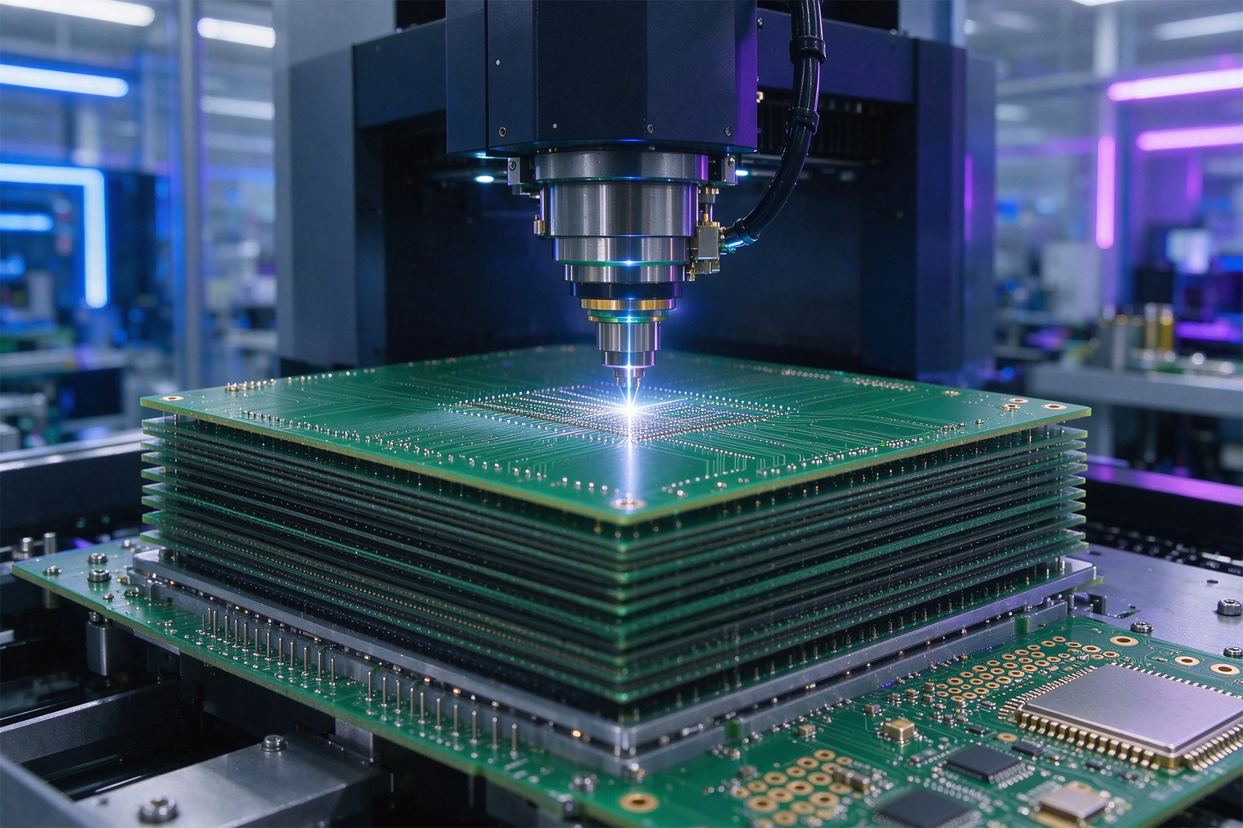
High frequency PCBs and HDI PCBs are both specialized categories that demand more from a fabrication facility than standard digital boards, but the requirements of each category overlap and interact in ways that create a distinct set of manufacturing challenges when they are combined.
High frequency boards require substrate materials that have specific, stable dielectric properties across the frequency range of operation. Common High Frequency Materials include Rogers Ro4003c, RT/duroid 5880, and similar ceramic-filled hydrocarbon or Ptfe substrates from specialty laminate manufacturers. These materials have dielectric constants that are engineered to be stable with frequency, in contrast to standard Fr-4, whose Dielectric Constant varies significantly across the frequency spectrum. The Dielectric Constant determines the propagation velocity and the wavelength of signals on the board, and variations in the dielectric constant, whether from material lot differences, temperature changes, or process variations, directly affect the impedance and the electrical performance of the board. An HDI manufacturer supporting high frequency projects must be able to process these specialty materials with the same precision and consistency as standard materials.
HDI boards, which are defined by the use of microvias with diameters of 0.15mm or smaller and by the fine-line circuitry that connects them, require manufacturing capabilities that are at the leading edge of PCB Fabrication technology. The microvia formation process, whether by laser drilling or by sequential build-up lamination, must produce vias with controlled diameter, controlled depth, and clean walls without resin smear or heat damage. The trace and space geometry of HDI boards, typically 75 microns or finer, requires precise etching control and careful process management to achieve the target conductor dimensions within tolerance. The lamination process for HDI boards, which may involve multiple build-up layers and multiple lamination cycles, must be controlled to prevent delamination, void formation, and layer-to-layer misalignment.
When high frequency and HDI requirements are combined, the manufacturer must manage the interactions between the material properties and the process parameters that affect both. The microvia formation process on High Frequency Materials, particularly Ptfe-based substrates, requires different process parameters than on standard materials. PTFE is a difficult material to drill with lasers because it does not ablate cleanly like standard epoxy-glass; it requires specialized laser parameters and often an initial plasma desmear step to clean the via walls and remove the heat-affected zone. The lamination process for HDI build-up on high frequency core materials must be controlled to prevent the high-Tg or high-flow prepreg from flowing into and contaminating the high-frequency signal layers. These interactions require a manufacturer who has specific experience with both HDI processes and high frequency materials.
The foundation of a successful high frequency HDI project is the proper handling, storage, and qualification of the high frequency substrate materials throughout the manufacturing process. These materials have different properties and different requirements than standard Fr-4, and the manufacturer's quality system must address these differences from the point of material receipt to the point of shipment.
Material incoming inspection for high frequency substrates must verify that the dielectric constant and the loss tangent of the received material match the specifications on the material datasheet. The fabricator should perform dielectric constant verification using a resonant cavity or a stripline test method on representative samples from each lot of material received. The test results should be documented and compared against the material specification to verify that the material lot is within the acceptable Dk range. This incoming verification provides the traceability that confirms the material in the production panel has the electrical properties that the design simulation assumed. A manufacturer who skips the incoming dielectric verification is accepting the risk that a material lot with out-of-specification properties will be used in production, resulting in boards that do not meet the impedance targets.
Material storage and handling for high frequency substrates must prevent moisture absorption, contamination, and physical damage that could affect the electrical or mechanical properties. PTFE-based materials, in particular, are susceptible to moisture absorption that can cause delamination during lamination or reflow, and they must be stored in a dry environment and dried before processing if they have been exposed to humidity. The manufacturer's storage procedures should include dry storage for moisture-sensitive materials, contamination-free handling practices that prevent fingerprint contamination or chemical exposure, and inspection protocols that detect any physical damage to the material panels before they enter the production process.
The stack-up design for a high frequency HDI board must be developed in collaboration between the customer and the manufacturer, because the achievable dielectric thicknesses and the available material grades depend on the manufacturer's material inventory and process capabilities. The manufacturer should provide a recommended stack-up that achieves the target impedance values using the dielectric thicknesses and materials that they can reliably produce, and the customer should use this manufacturer-recommended stack-up as the basis for the impedance simulation rather than attempting to derive a theoretical stack-up that may not be producible. The collaboration on stack-up design is particularly important for HDI boards, where the thin dielectric layers required for the microvia structure may conflict with the dielectric thickness required for the Controlled Impedance traces.
The microvia is the defining feature of HDI technology, and its formation on high frequency substrate materials requires specialized process capabilities that not all HDI manufacturers possess. The laser drilling process that creates microvias must be optimized for the specific high frequency material being used, and the process parameters must be controlled to ensure consistent via quality across the panel and across production lots.
Laser drilling of PTFE-based high frequency materials presents a specific challenge that is not encountered with standard epoxy-glass substrates. PTFE does not absorb the CO2 laser wavelength efficiently, which means that the ablation process is less controlled and more heat is generated at the via walls. The heat-affected zone, the region of thermally degraded material around the via wall, can affect the dielectric properties near the via and can interfere with the plating process by creating a poor bonding surface for the copper. The manufacturer's laser drilling process for PTFE materials should include parameters that minimize the heat-affected zone, including multiple low-energy pulses rather than a single high-energy pulse, and the process should be verified through microsection examination of the via walls to confirm that the HAZ is within acceptable limits.
Via desmear and activation for high frequency materials, particularly for the sequential build-up layers in HDI boards, must use chemistry that does not attack or degrade the base substrate material. The standard permanganate desmear process used for FR-4 boards can be too aggressive for some high frequency materials, particularly those with ceramic fillers that may be partially dissolved by the alkaline permanganate solution. The manufacturer should use a desmear process that is specifically qualified for the high frequency material being processed, which may include plasma desmear, which is a dry process that avoids the chemical exposure of wet desmear, or a modified wet desmear with reduced process time or modified chemistry. The desmear process should be verified by microsection examination to confirm that the via walls are clean and that the dielectric material is not degraded.
Via filling and planarization for high frequency HDI boards must achieve a flat surface for the subsequent build-up layers without introducing voids or surface irregularities that could affect the fine-line photolithography of the next layer. The via fill material, whether a conductive copper fill or a non-conductive via fill, must be compatible with the high frequency substrate and must not outgas or decompose during the subsequent lamination cycles. The planarization process, which may use mechanical grinding or chemical-mechanical polishing, must remove the fill material to the correct depth without damaging the surrounding copper or the dielectric surface. The manufacturer should provide process capability data for the via fill and planarization process, including microsection data that shows the fill quality and the surface flatness across the panel.
The impedance of the Transmission Lines on a high frequency HDI board must be controlled to tighter tolerances than on a standard digital board, because the Signal Integrity at high frequencies is more sensitive to impedance deviations. The trace geometry, the dielectric thickness, and the dielectric constant must all be controlled simultaneously to achieve the target impedance within the specified tolerance.
The trace width control for high frequency boards, particularly for the fine-line traces used in HDI circuitry, requires tighter process control than standard boards because the impedance is directly proportional to the trace width for a Microstrip trace. A 10 percent variation in trace width on a 50 ohm Microstrip produces approximately a 5 ohm impedance variation, which may exceed the specified tolerance for the application. The manufacturer should apply etch compensation to the artwork, adjusting the drawn trace width to account for the lateral etch that occurs during the etching process, so that the finished trace width matches the target. The etch compensation values should be based on process capability data for the specific material, copper weight, and trace geometry, and the manufacturer should provide statistical process control data that demonstrates the achieved trace width tolerance.
The dielectric thickness control for high frequency HDI boards is more challenging than for standard boards because the HDI build-up process involves multiple thin dielectric layers that must be laminated without thickness variation or void formation. The dielectric thickness between the signal layer and the reference plane determines the impedance for a microstrip trace, and a 10 percent variation in dielectric thickness produces approximately a 5 percent variation in impedance. The manufacturer should provide statistical process control data for the dielectric thickness of the high-frequency-critical layers, including the thickness variation within a panel and the panel-to-panel variation. The dielectric thickness should be measured by microsection at multiple locations across the panel to characterize the within-panel uniformity.
The Characteristic Impedance of Transmission Lines on HDI boards is affected by the proximity of the traces to each other and to other copper features, which creates coupling effects that are not present on isolated single traces. The coupling between adjacent microstrip traces, which is described by the odd-mode and even-mode impedances, depends on the trace spacing as well as the trace width and dielectric thickness. For high frequency HDI boards with dense routing, the coupling effects must be included in the impedance calculation, and the manufacturer must control the trace spacing with the same precision as the trace width. The coupling effects are particularly important for differential pair routing, where the differential impedance depends on the odd-mode impedance, which is directly affected by the trace spacing.
The surface finish on a high frequency HDI board affects the conductor loss, the solderability, and the shelf life of the finished board, and the surface finish selection must balance these requirements against the constraints of the HDI process and the high frequency requirements.
ENIG, electroless nickel immersion gold, is the most common surface finish for high frequency boards because it provides a flat, uniform surface that is compatible with fine-pitch component assembly and because the gold layer protects the underlying nickel from oxidation. The nickel layer in ENIG, which is typically 3 to 6 microns thick, has higher resistivity than copper, which adds a small series resistance to the signal path and increases the conductor loss at high frequencies. For very high frequency applications, above approximately 10 GHz, the nickel resistance contribution may be significant enough to justify alternative surface finishes. The ENIG process must be carefully controlled to prevent black pad, a nickel corrosion condition that causes poor solderability and that is particularly problematic for the fine-pitch pads of HDI boards.
Immersion silver provides a thin, flat surface with lower conductor loss than ENIG because the silver layer is thinner and has lower resistivity than the nickel-gold combination. The silver layer, typically 0.1 to 0.2 microns thick, is too thin to provide significant wire bondability or long-term corrosion protection, but it is adequate for solder assembly and it preserves the high frequency signal quality better than ENIG. The shelf life of immersion silver is limited compared to ENIG, typically 6 to 12 months in dry storage, because the silver surface tarnishes in the presence of airborne sulfur compounds. The manufacturer should specify the shelf life and the storage requirements for immersion silver boards, and the customer should plan the assembly timeline accordingly.
OSP, organic solderability preservative, provides a thin protective coating over the copper surface that preserves solderability without adding significant thickness or conductivity to the conductor. OSP is compatible with fine-pitch assembly and is one of the lowest-cost surface finishes, but it has limited shelf life and is not suitable for boards that will be stored for extended periods before assembly. OSP is also not compatible with multiple reflow cycles or with boards that require touch-up soldering after the initial assembly, because the OSP coating is consumed during the first reflow. For high frequency HDI boards that will be assembled promptly after receipt, OSP may be a cost-effective surface finish choice, but the limited rework capability and the storage constraints should be evaluated against the application requirements.
The layer registration accuracy of HDI boards, which is the precision with which each build-up layer is aligned with the layers below it, must be controlled more tightly than for standard multilayer boards because the microvia capture pads are smaller and the tolerance for layer-to-layer misalignment is correspondingly tighter. The registration error budget for a high frequency HDI board must account for the cumulative effect of the registration errors at each build-up layer.
The lamination process for HDI boards must be controlled to prevent layer-to-layer shift, which is the relative movement of the build-up layers relative to the core layers during the lamination pressure and temperature cycle. The lamination pressure, temperature ramp rate, and the degree of vacuum applied during lamination all affect the layer-to-layer shift, and the manufacturer's process parameters must be optimized for the specific HDI construction and the specific material set. The manufacturer's process qualification should include registration measurements on test panels that are built with the same stack-up and lamination parameters as the production panels, measuring the layer-to-layer registration at the corners, the edges, and the center of the panel.
The optical alignment system used for the photolithography of each build-up layer must be capable of aligning to the underlying circuitry with sufficient accuracy to ensure that the microvia lands are properly positioned relative to the target pads on the layer below. The alignment system typically uses fiducial marks on the panel surface and on the artwork to compute the panel distortion and to adjust the exposure pattern accordingly. For high frequency HDI boards with tight microvia tolerances, the alignment system must have resolution of 10 microns or better, and the process must be validated by measuring the actual microvia position relative to the target pad after the via is drilled and the subsequent layer is imaged.
The build-up sequence for a high frequency HDI board with multiple sequential build-up layers must be planned to minimize the cumulative registration error and to preserve the electrical performance of the high-frequency-critical layers. The outermost high-frequency signal layers, which typically carry the RF signals at the highest frequencies, should be placed as close to the outer surface as possible to minimize the number of build-up layers and the associated registration errors between the signal layer and the antenna or connector interface. The internal high-frequency layers, if present, should be protected from the process steps of the subsequent build-up layers to prevent damage or contamination that could affect the dielectric properties.
The testing requirements for high frequency HDI boards extend beyond the standard continuity and isolation tests used for standard digital boards, because the electrical performance at high frequencies depends on parameters that are not verified by standard testing. The manufacturer must have the test capability and the test methodology to verify the impedance, the dielectric properties, and the RF performance of the delivered boards.
Impedance testing using time-domain reflectometry verifies that the Characteristic Impedance of the transmission lines is within the specified tolerance. The Tdr test launches a fast step pulse into the Transmission Line and measures the reflected pulse, which indicates the impedance at each point along the line. For high frequency HDI boards, the Tdr test should be performed on impedance test coupons that are fabricated on the same panel as the production boards and that have the same stack-up and trace geometry as the production traces. The test coupon design should include representative trace geometries for each impedance target on the board, including single-ended traces, differential pairs, and any coupled-line structures that are used in the design. The TDR measurement should be performed with sufficient bandwidth to resolve the impedance variations that are relevant at the operating frequency.
Cross-sectional analysis, also called microsection analysis, verifies the internal structure of the HDI board, including the microvia quality, the dielectric thickness, the layer alignment, and the plating integrity. The microsection is prepared by cutting a representative sample from the board, mounting it in epoxy, grinding and polishing the cut surface to the plane of interest, and examining it under a microscope. For high frequency HDI boards, the microsection should be examined at the high-frequency-critical layers to verify the dielectric thickness, the trace width, the trace geometry, and the microvia quality including the plating thickness and the absence of voids or cracks. The microsection results should be documented with photographs and measurements that can be compared against the acceptance criteria.
Insertion Loss measurement, which quantifies the Signal Loss as it propagates through the Transmission Line, is the most direct verification of the high frequency electrical performance of the board. The Insertion Loss includes the conductor loss, which depends on the trace width, the copper roughness, and the Skin Effect at high frequencies, and the dielectric loss, which depends on the loss tangent of the substrate material and the operating frequency. The insertion loss is measured using a vector network analyzer with a frequency-domain measurement that covers the operating frequency range of the board. For high frequency HDI boards, the insertion loss budget should be allocated among the various loss contributors, and the measured insertion loss of the production boards should be compared against the budget to verify that the total loss is within the acceptable limit.
The successful execution of a high frequency HDI project requires a level of collaboration between the customer and the manufacturer that goes beyond the typical customer-supplier relationship for standard PCB orders. The design decisions that are made early in the project, including the stack-up, the via strategy, the routing rules, and the test coupon design, have a lasting impact on the manufacturing cost and the electrical performance, and these decisions should be made in consultation with the manufacturer's engineering team.
Stack-up design collaboration ensures that the board stack-up is both electrically correct and manufacturing-feasible. The customer provides the impedance targets, the frequency range, and the layer count requirements, and the manufacturer provides the available dielectric thicknesses, the material grades in their inventory, and the process capability data for the critical dimensions. Together they develop a stack-up that achieves the impedance targets using the available materials and processes, with appropriate margins to account for the manufacturing tolerances. The collaboration should include a review of the impedance simulation results using the manufacturer's verified dielectric constant values, rather than the datasheet nominal values, to ensure that the simulation accurately predicts the manufactured impedance.
Via strategy development, which determines the via types and the via locations for the board, should be a collaborative process because the via choices affect both the electrical performance and the manufacturing cost. The microvia strategy for HDI boards, including whether to use staggered microvias or stacked microvias, whether to use via-in-pad or dog-bone routing, and whether to fill the microvias or to leave them as through-holes, has trade-offs that the manufacturer is best positioned to explain. The blind and buried via strategy, if the board uses these via types, should be developed in consultation with the manufacturer to ensure that the via structure is compatible with the build-up process and the lamination sequence.
Dfm review, where the manufacturer's engineering team reviews the customer's design data for manufacturability issues before the fabrication begins, is a standard service that reputable HDI manufacturers provide for high frequency projects. The Dfm review covers the trace width and spacing tolerances, the via aspect ratios, the annulus dimensions, the solder mask coverage over high-frequency features, and the test point accessibility. The review should be documented in a DFM report that identifies each issue, classifies it by severity, and recommends a specific resolution. The customer should have the opportunity to discuss the DFM findings with the manufacturer's engineering team and to revise the design before the fabrication files are released for production.
High frequency HDI boards used in regulated industries, including aerospace, defense, medical, and automotive, must meet specific certification and compliance requirements that go beyond the standard IPC acceptance criteria. The manufacturer must have the quality system certifications, the process controls, and the documentation practices that support compliance with these requirements.
AS9100 certification for aerospace applications, ISO 13485 certification for medical applications, and IATF 16949 certification for automotive applications are Quality Management System standards that define the requirements for the design, development, production, and delivery of products in their respective industries. A manufacturer with these certifications has demonstrated that they have the quality management infrastructure, the process controls, and the documentation practices that are required for regulated industry supply. For high frequency HDI projects in these industries, the manufacturer should hold the appropriate certification and should be willing to provide evidence of the certification status, including the certificate number and the scope of the certification.
First Article Inspection per AS9102 provides a standardized format for documenting the first article inspection results, including the dimensional measurements, the material verification, and the functional test results. The FAI documentation package includes the inspection results for each characteristic on the engineering drawing, the material certificates for the raw materials, and the process parameters for the critical manufacturing steps. For high frequency HDI boards, the FAI should include the impedance test results, the microsection results, and any RF performance measurements that are specified in the acceptance criteria. The FAI package should be reviewed and accepted by the customer's quality organization before the production run is authorized to proceed beyond the first article quantity.
Lot traceability for high frequency HDI boards used in regulated industries must provide the ability to trace each finished board back to the specific lots of raw material, the specific manufacturing processes, and the specific inspection results that were used to produce it. The manufacturer's traceability system should record the material lot numbers for each substrate material, prepreg, and copper foil used in each panel, the process parameters for each manufacturing step, and the inspection and test results for each board. The traceability records should be retained for the period required by the applicable industry regulation, which may be 10 years or longer for aerospace and medical applications.
The capabilities required to support high frequency HDI projects are not evenly distributed across the Pcb Manufacturing industry. Engineers and procurement professionals who are evaluating manufacturers for these projects should assess the specific capabilities that are most critical for their application, rather than relying on general claims of HDI or high frequency capability.
Equipment assessment should verify that the manufacturer has the specific equipment required for high frequency HDI production, including laser drilling systems capable of producing microvias in high frequency materials, lamination systems with precise temperature and pressure control for HDI build-up, impedance test systems with adequate bandwidth for the target frequency range, and cross-section equipment for microsection analysis. The equipment should be maintained and calibrated according to a documented maintenance schedule, and the manufacturer should be willing to provide evidence of the equipment calibration status. A manufacturer who outsources some of these processes to secondary vendors may not have the same level of process control as one who performs all of the critical processes in-house.
Process capability data should be requested to demonstrate the manufacturer's ability to achieve the tolerances required for the specific project. The data should include statistical process control charts for the critical dimensions, including trace width, dielectric thickness, and impedance, for representative board types that are similar to the project being quoted. The Cpk values, which quantify the process capability as the ratio of the tolerance width to the process spread, should be 1.33 or higher for critical dimensions, which indicates a capable process that consistently produces parts within tolerance. A manufacturer who cannot provide process capability data for the dimensions that are most critical to the project may not have the process control needed for high frequency HDI production.
Sample evaluation, where the manufacturer produces a small number of prototype boards that are tested and evaluated before the production commitment, is the most reliable method for verifying the manufacturer's capability for a specific high frequency HDI project. The sample boards should be tested to the same acceptance criteria that will be applied to the production boards, including impedance testing, microsection analysis, and any RF performance measurements. The sample evaluation provides the opportunity to identify any capability gaps or process issues before the production quantity is committed, reducing the risk of a costly production escape. A manufacturer who is confident in their high frequency HDI capability should be willing to produce samples at a competitive price and should stand behind the results of the sample evaluation.
High frequency Hdi Pcb projects are among the most demanding in the PCB industry, requiring a manufacturer who combines the Precision Manufacturing capabilities of HDI technology with the material expertise and process control of high frequency fabrication. The intersection of these two disciplines creates specific challenges in material handling, microvia formation, Impedance Control, and layer registration that must be addressed with specialized equipment, optimized process parameters, and rigorous quality control.
The selection of a manufacturing partner for high frequency HDI projects should be based on a demonstrated capability in both disciplines, not just a general claim of HDI or high frequency expertise. The evaluation should include an assessment of the equipment, the process capability data, the material handling procedures, and the quality system certifications that are relevant to the specific application. The most reliable verification of capability is the sample evaluation, where the manufacturer demonstrates the actual results that can be achieved on the specific project before the production commitment is made.
Contact us to discuss your high frequency HDI project requirements and to explore how our manufacturing capabilities support demanding RF and microwave applications with HDI interconnection density.
How to Evaluate a High Frequency PCB ManufacturerOctober/26/2026
Case Study: How the Right High Frequency PCB Manufacturer Solved a Critical EMI IssueSeptember/09/2026

Why Certifications Matter: IATF16949 and ISO Standards for Your High Frequency PCB ManufacturerJune/17/2026

How High Frequency PCB Applications are Powering the AI Server RevolutionAugust/03/2026
7 Key Factors to Consider When Choosing a High Frequency PCB ManufacturerMay/29/2026
From Prototype to Mass Production: Scaling with a Reliable High Frequency PCB ManufacturerJuly/13/2026

What to Ask a High Frequency PCB Manufacturer Before QuotingNovember/10/2026
Top 5 Questions to Ask Your High Frequency PCB Manufacturer Before Placing an OrderAugust/14/2026