Open Nav

Rf Design lives and dies by material properties. A filter that sims perfectly with a Dk of 3.0 shifts its center frequency 5% when the actual board Dk turns out to be 3.15. A power amplifier that delivers 40dBm at 2.4GHz on paper loses 2dB of output when the substrate loss tangent is twice what you assumed. These are not hypothetical problems—they happen routinely when designers pick Pcb Materials by brand name rather than by measured parameters matched to their specific frequency and application requirements. The PCB substrate determines impedance accuracy, Insertion Loss, radiation efficiency, and thermal behavior of every RF circuit on the board. Choosing the wrong material does not just degrade performance; it can make the design unworkable at any reasonable tuning effort. This article provides a systematic framework for selecting high frequency PCB materials for RF designs, with practical comparisons and decision criteria that go beyond datasheet numbers.
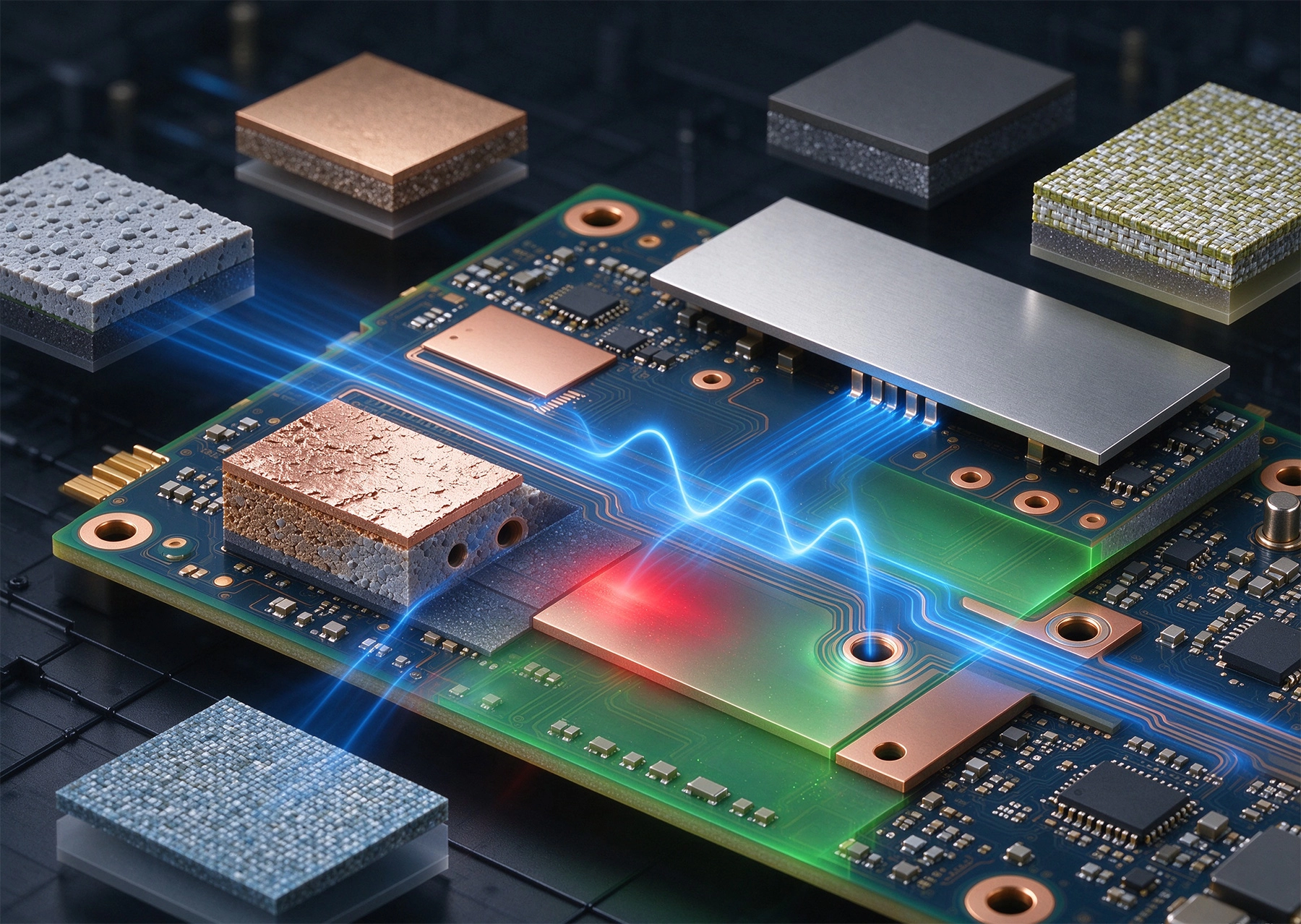
Before comparing specific materials, you need to understand which parameters drive RF performance and which are secondary distractions. Many designers focus on Dielectric Constant (Dk) alone, but for RF work, several parameters interact to determine circuit behavior.
Dk determines the wavelength and impedance of traces on the PCB. For Microstrip and stripline Transmission Lines, the Characteristic Impedance depends directly on the square root of the effective Dk. A 10% change in Dk produces roughly a 5% change in impedance—enough to degrade return loss by several dB in a narrowband design.
But raw Dk value is only part of the story. What matters for Rf Design is:
Loss tangent quantifies how much RF energy the dielectric absorbs per cycle. It directly determines Insertion Loss per unit length of Transmission Line. The relationship is approximately: insertion loss (dB/inch) ∝ frequency × Dk^0.5 × Df. This means loss tangent impact scales linearly with frequency—what is negligible at 100MHz becomes dominant at 10GHz.
Practical impact of loss tangent at different frequencies:
Moisture absorption affects both Dk and Df. Water has a Dk of about 80 and a very high loss tangent. Even small amounts of absorbed moisture shift the composite Dk upward and increase loss. Standard FR-4 absorbs 0.1–0.2% moisture by weight; Ptfe-based laminates absorb less than 0.02%. For RF designs that must maintain performance across humid environments—which is most outdoor and defense applications—moisture absorption is a critical selection criterion.
CTE matters for RF designs that use lead-free solder assembly and must survive thermal cycling. A large CTE mismatch between the laminate and copper causes via barrel cracking and pad lifting. For RF boards with many via fences (common around RF switches and amplifier stages), via reliability under thermal stress is a real concern. Ptfe-based materials have high z-axis CTE (200+ ppm/°C), which is a significant reliability risk for plated through holes in thick boards. Ceramic-filled PTFE laminates (like Rogers RO3003) reduce z-axis CTE to more manageable levels.
high frequency PCB materials fall into several families, each with distinct performance, processing, and cost characteristics. Understanding these families is more useful than memorizing individual part numbers.
Standard FR-4 (epoxy-glass, brominated flame retardant) has Dk around 4.3–4.6 and Df around 0.015–0.020 at 1MHz. At RF frequencies, effective Dk drops to about 4.2–4.4 and Df rises to 0.020–0.030.
Where FR-4 works for RF:
Where FR-4 fails for RF: Narrowband filters, low-noise amplifier input matching, power amplifier output networks, phased array feed networks, and any circuit where insertion loss or Dk stability directly limits system performance. High-TG FR-4 variants (Isola 370HR, Megtron 6) improve thermal reliability and slightly reduce loss but dont fundamentally change the RF performance picture.
These materials use standard epoxy or phenolic resin systems loaded with ceramic fillers to reduce loss tangent and stabilize Dk. They process like FR-4—same drill speeds, same lamination profiles, same etch chemistry—which makes them the easiest Low-loss Materials to adopt.
Examples and characteristics:
When to choose this category: 1–10GHz applications where you need significantly lower loss than FR-4 but cannot justify the processing complexity and cost of PTFE materials. This covers most Wi-Fi, cellular, and mid-band RF designs.
PTFE (polytetrafluoroethylene) based laminates offer the lowest loss tangents available—0.0004 to 0.002 at 10GHz. They are the material of choice for demanding RF applications but come with significant manufacturing challenges.
Key PTFE laminates:
Manufacturing challenges with PTFE:
When to choose PTFE: Applications above 10GHz, defense/aerospace radar and EW systems, Satellite Communications, and any design where insertion loss budget cannot be met with modified epoxy materials. If you can achieve your loss target with RO4003C, you should—PTFE only when you must.
Ceramic-based laminates fill a niche between modified epoxy and PTFE:
These materials offer a middle ground—lower loss than modified epoxy, easier processing than PTFE—but availability can be limited and not all fabricators have experience with them.
Choosing an Rf Pcb material is not a single decision—it is a sequence of elimination steps based on your specific requirements. Here is a practical framework.
Before looking at any material datasheet, quantify what your design actually needs:
Using your requirements from Step 1, eliminate material families:
From the remaining candidates, filter by practical considerations:
Datasheet Dk and Df values are measured under specific test conditions (usually clamped stripline resonator at a few GHz). Your actual circuit—microstrip on a specific stack-up thickness at your operating frequency—will see different effective values. Before committing to production:
Many practical RF boards do not need low-loss material on every layer. A typical RF design has critical Transmission Lines on one or two layers and digital/power routing on the rest. A hybrid stack-up uses different materials for different layers, placing Low-loss Laminate only where the RF signals actually route.
Hybrid stack-ups introduce issues that homogeneous stack-ups do not:
Different RF applications prioritize different material properties. Here is how to think about material selection for common RF design types.
PA output matching is extremely loss-sensitive. Every 0.1dB of loss in the output matching network directly reduces PAE (power-added efficiency) and output power. At 2–6GHz cellular bands, modified epoxy materials (RO4003C) are usually adequate for handset PAs where trace lengths are short. For base station PAs with longer matching networks and higher power levels, ceramic-filled PTFE (RO3003) is often necessary. The material must also handle the thermal dissipation from the PA die—thermal conductivity of the laminate matters here, not just dielectric loss.
Phased arrays require exceptional Dk uniformity. All antenna elements must see the same effective electrical length to their respective feed points, or beam pointing accuracy and sidelobe levels degrade. Dk variation of ±0.05 across a panel can cause several degrees of beam pointing error in a large array. Materials with tight Dk tolerance (Rogers RO4003C at ±0.05, RT/duroid 5880 at ±0.02) are essential. For mmWave arrays at 28–39GHz, PTFE-based materials are the only practical choice.
Filters are the most Dk-sensitive Rf Circuits. A bandpass filter with 5% bandwidth centered at 3GHz shifts its center frequency by 75MHz for every 1% change in Dk. For a filter that must meet a tight spectral mask, that shift can push the filter out of specification. Material selection for filters should prioritize Dk stability (both lot-to-lot and over temperature) above loss tangent. A slightly higher loss material with rock-solid Dk stability often produces a more manufacturable filter than a lower-loss material with Dk variation.
LNA input matching networks are loss-sensitive in a different way than PA output networks—here, loss directly adds to the noise figure. A 0.1dB loss before the first LNA degrades the entire receivers noise figure by 0.1dB. For LNA input networks at frequencies above 3GHz, low-loss material is worthwhile even for short trace lengths. Below 3GHz, the loss contribution is small enough that FR-4 may be acceptable if the LNA is not the system noise bottleneck.
Material cost per square foot is only part of the total cost equation. Here is a realistic comparison for a 6-layer, 4″ × 6″ board at moderate volume (100 pieces):
The hybrid approach often provides the best cost-performance ratio for practical RF designs. Saving 40–60% on board cost while getting identical RF performance on the critical layers is compelling. The constraint is that your fabricator must be comfortable with mixed-dielectric lamination—which most mid-capability fabricators are for modified epoxy/FR-4 hybrids, but not necessarily for PTFE/FR-4 hybrids.
Selecting the right high frequency pcb material is not about finding the lowest loss tangent at any cost. It is about matching material properties to your specific RF requirements while staying within your manufacturing capability and budget constraints. The best material for your design is the one that meets your electrical requirements with margin, can be reliably processed by your fabricator, and fits your cost envelope. Everything else is over-specification or under-specification—and both have consequences.
Contact us to discuss your requirements
Understanding Thermal Stability in High Frequency PCB MaterialsAugust/10/2026
Cost vs. Performance: Selecting Budget-Friendly High Frequency PCB MaterialsSeptember/04/2026

Top 5 High Frequency PCB Materials for 5G Base Station ApplicationsJuly/30/2026
The Impact of Copper Foil Type on High Frequency PCB Materials PerformanceSeptember/16/2026
Choosing the Right High Frequency PCB MaterialsMay/29/2026
High Frequency PCB Materials for Automotive Radar: Durability and SpeedSeptember/26/2026
How Dielectric Constant (Dk) and Loss Factor (Df) Affect High Frequency PCB MaterialsJuly/18/2026
Emerging Trends in High Frequency PCB Materials for Next-Gen CommunicationOctober/10/2026