Open Nav

Designing circuits for radio frequency and microwave applications demands a fundamentally different approach to Pcb Material Selection than digital circuit design. At low frequencies, the substrate material is largely irrelevant to circuit performance; a piece of cardboard with copper traces would function almost identically to an expensive engineered laminate. At 10 GHz, 28 GHz, or 77 GHz, the material properties determine whether the circuit works at all. The Dielectric Constant controls propagation velocity and impedance. The Dissipation Factor controls how much signal is lost as heat. The combined effect of these properties determines whether your Rf Design meets its performance targets or falls short in ways that may not be obvious until the prototype is tested. Understanding these material properties, and how they behave across frequency and temperature, is the foundation for making informed high frequency PCB material selections.
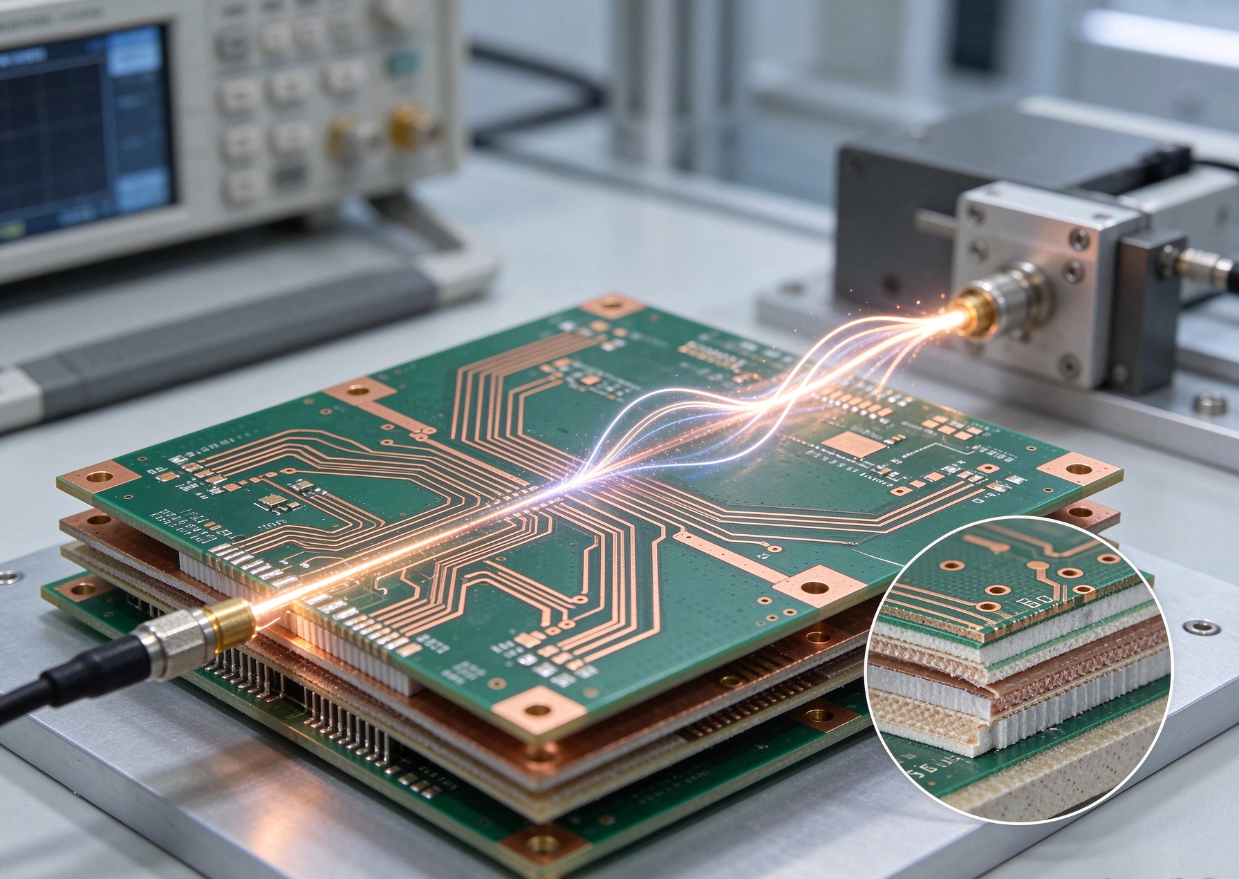
The Dielectric Constant, often called relative permittivity or simply Dk, describes how the PCB substrate material affects the electric field within the board. When a signal propagates along a Transmission Line on a PCB, the electric field extends partly into the substrate, and the substrate material determines how quickly the field can establish itself. A higher dielectric constant means the field is more constrained, the effective capacitance between the trace and the reference plane increases, and the propagation velocity decreases. The relationship between propagation velocity and dielectric constant is inversely proportional: doubling the dielectric constant halves the propagation velocity.
For Controlled Impedance designs, the dielectric constant determines the trace geometry required to achieve the target impedance. A 50-ohm Microstrip trace on a substrate with Dk of 4.0 requires different dimensions than the same trace on a substrate with Dk of 3.0. If the actual dielectric constant of the manufactured board differs from the design assumption, the manufactured impedance will differ from the target. For narrowband applications, small impedance errors may be tolerable. For wideband applications or designs with critical matching networks, impedance errors cause reflection, poor matching, and degraded performance.
The dielectric constant is not a fixed property but varies with frequency. This frequency dependence, called dispersion, means that the Dk measured at one frequency may not apply at another. Some materials have relatively flat Dk versus frequency behavior, meaning they maintain nearly the same Dk across a wide range. Others exhibit significant Dk variation, which complicates design for wideband applications. When selecting materials for high frequency use, look for data on Dk at the actual frequency of operation, not just the datasheet value which may be specified at a lower frequency.
The Dissipation Factor, also called loss tangent or Df, quantifies how much energy is lost when the PCB material is subjected to alternating electric fields. When a signal propagates through a lossy dielectric, a portion of the signal energy is absorbed by the material and converted to heat. The fraction lost per unit distance depends on the Df and the frequency. Higher Df means more loss. Higher frequency also means more loss, approximately proportionally, for a given Df.
The practical consequence of dissipation factor is Insertion Loss. In a Transmission Line, the signal power at the output is less than the signal power at the input due to losses along the path. These losses come from two sources: conductor loss from the resistance of the copper traces, and dielectric loss from the substrate. At low frequencies, conductor loss dominates. At high frequencies, dielectric loss becomes increasingly significant, and for some materials at millimeter-wave frequencies, dielectric loss dominates entirely.
For power amplifier applications, dielectric loss matters because it reduces efficiency. A power amplifier that delivers 10 watts to the load but loses 2 watts to dielectric heating in the matching network and Transmission Lines is less efficient than one that loses only 0.5 watts. Lower efficiency means more heat, shorter battery life, and higher operating costs. For receive applications, dielectric loss matters because it reduces the signal level reaching the low-noise amplifier, degrading the signal-to-noise ratio and reducing range or sensitivity.
Comparing typical Df values illustrates why material selection matters. Standard FR4 has Df in the range of 0.015 to 0.025 at GHz frequencies. Rogers Ro4003c, a popular High Frequency Laminate, has Df of approximately 0.0027 at 10 GHz. Rogers RT/duroid 5880, a Ptfe material, has Df of approximately 0.0009 at 10 GHz. At 28 GHz, the dielectric loss in FR4 is approximately 5 to 8 times higher than in RT/duroid 5880, which translates directly to a significantly shorter propagation distance before the signal is unacceptably attenuated.
The total loss in a PCB transmission line is the sum of conductor loss and dielectric loss. Conductor loss arises from the finite conductivity of copper and the Skin Effect, which forces alternating current to flow in a thin layer near the conductor surface. As frequency increases, the skin depth decreases, the effective cross-sectional area decreases, and the resistance increases. Conductor loss scales roughly with the square root of frequency due to the Skin Effect.
Dielectric loss scales approximately linearly with frequency for a given material. At low frequencies, dielectric loss may be negligible compared to conductor loss. At high frequencies, dielectric loss can dominate. The frequency at which dielectric loss becomes significant depends on the Df of the material. High-Df materials like FR4 exhibit significant dielectric loss at frequencies above a few GHz. Low-Df materials like Ptfe can maintain low dielectric loss up to Millimeter Wave frequencies.
For Transmission Lines carrying high-frequency signals over meaningful distances, dielectric loss often dominates. A 10 cm Microstrip line on FR4 at 28 GHz might have total loss dominated by dielectric effects, while the same line on RT/duroid 5880 might have losses dominated by conductor effects because the dielectric loss is so low. This means that switching from FR4 to a low-Df material can dramatically improve Insertion Loss, but only if the conductor loss is also controlled through appropriate trace geometry and surface finish.
The surface roughness of the copper conductor adds another loss mechanism. Rough copper increases conductor losses because the high-frequency current follows the rough surface contours, increasing the effective path length and resistance. For standard PCB copper with RMS roughness of 1 to 2 microns, the additional loss at 10 GHz is modest. At higher frequencies like 28 or 77 GHz, surface roughness loss becomes more significant, and smoother copper finishes may be beneficial for low-loss applications.
The frequency dependence of dielectric properties affects design accuracy and manufacturing consistency. Materials with stable Dk and Df across frequency simplify design because the values used in simulation apply across the operating band. Materials with significant frequency dependence require designers to account for property variation, either by using frequency-specific values in simulation or by accepting some performance variation across the band.
Temperature dependence is equally important for applications where the PCB will experience temperature variation. The dielectric constant and dissipation factor of most materials vary with temperature, a property called the thermal coefficient of dielectric constant, or TCDk. For frequency-critical applications, the TCDk determines how much the dielectric properties will drift as temperature changes, which translates directly to drift in propagation velocity and impedance.
PTFE-based materials generally have excellent temperature stability, with very low TCDk values that maintain consistent dielectric properties across wide temperature ranges. This stability makes PTFE attractive for applications like Satellite Communications where temperature extremes are large and performance consistency is critical. Hydrocarbon ceramic materials like Rogers RO4000 series have moderate TCDk values, better than FR4 but not as stable as PTFE. For applications where temperature stability matters but PTFE cost is prohibitive, the Rogers materials offer a reasonable compromise.
Humidity absorption also affects dielectric properties. Some materials absorb moisture from the environment, and water has a dielectric constant of approximately 80, much higher than typical Pcb Substrate Materials. When a material absorbs moisture, its effective Dk increases, which shifts impedance and propagation velocity. For outdoor or humid-environment applications, selecting materials with low moisture absorption or controlling the operating environment prevents performance drift from this mechanism.
The market for high frequency PCB materials includes several distinct families, each with characteristic properties, advantages, and limitations. Understanding these families helps narrow the material selection to a small set of candidates that can be evaluated for the specific application requirements.
Hydrocarbon ceramic laminates, exemplified by Rogers RO4000 series materials, offer a compelling balance of electrical performance, mechanical properties, and manufacturing accessibility. RO4003C with Dk of 3.38 and Df of 0.0027 at 10 GHz provides substantially better loss performance than FR4 while maintaining processing characteristics similar to standard FR4. These materials can be fabricated by many PCB manufacturers without the specialized equipment required for PTFE, making them more accessible and often more affordable for commercial applications.
PTFE composites with ceramic or glass fillers offer the best electrical performance among commonly available Pcb Materials. Rogers RT/duroid 5880 with Dk of 2.2 and Df of 0.0009 at 10 GHz provides extremely low loss suitable for the most demanding applications including aerospace, defense, and test equipment. The trade-off is manufacturing complexity: PTFE requires specialized drilling, desmearing, and plating processes that not all manufacturers can perform reliably. Boards built on PTFE materials typically cost more and have longer lead times than equivalent hydrocarbon ceramic boards.
FR4 and standard epoxy-glass laminates remain the appropriate choice for applications where high frequency performance is not critical. Many RF applications operate at frequencies where FR4 loss is acceptable, particularly for short interconnect distances where total insertion loss is low. For antenna feeds below 6 GHz with short runs, or for simple RF switching circuits, the cost and availability advantages of FR4 may outweigh its electrical disadvantages.
For applications where insertion loss is a primary concern, material selection is only part of the solution. The design of the transmission lines and matching networks also affects loss performance, and applying loss-minimizing design practices amplifies the benefits of Low-loss Materials.
Microstrip transmission lines are the most common RF interconnect on PCB. The loss in a microstrip line depends on trace width, substrate thickness, and material properties. Wider traces on thicker substrates have lower conductor loss because the current distributes over a larger cross-section. However, wider traces also have less coupling to the reference plane, which affects impedance and potentially increases radiation. Optimizing trace geometry for minimum total loss requires balancing these factors for the specific frequency and material.
Grounded Coplanar Waveguide, Gcpw, offers advantages for some high-frequency applications. Gcpw uses a Ground Plane on the same layer as the signal trace, with slots defining the signal channel, which provides better Shielding and reduces radiation loss compared to microstrip. GCPW also provides better heat dissipation from the signal trace, which can be beneficial for power applications. However, GCPW requires tighter manufacturing tolerances for the slot dimensions and may be more sensitive to manufacturing variation than microstrip.
Substrate integrated waveguide, SIW, is a transmission structure formed by rows of vias in a dielectric substrate, creating a waveguide-like structure with low loss at high frequencies. SIW is particularly attractive for millimeter-wave applications where the guided wavelength becomes small enough that SIW structures fit practically on a PCB. The loss in SIW can be lower than microstrip at very high frequencies because the electromagnetic field is more confined and radiation losses are reduced.
The appropriate material selection depends on a systematic evaluation of what the application actually requires. Over-specifying material requirements wastes cost; under-specifying material requirements risks performance failures. A structured evaluation process identifies the minimum acceptable material performance and then selects the lowest-cost material that meets those requirements.
For cellular infrastructure applications in the sub-6 GHz range, hydrocarbon ceramic materials like Rogers Ro4350b or RO4003C are typically the right choice. The operating frequencies, the moderate distances over which signals must propagate, and the cost sensitivity of commercial infrastructure equipment all align well with these materials. More exotic materials like PTFE would provide marginal performance benefit at unacceptable cost for these high-volume applications.
For Automotive Radar at 77 GHz, the frequency is so high and the loss budget is so tight that PTFE-based materials or the lowest-loss hydrocarbon ceramics are required. The automotive environment also demands reliability under extreme temperature cycling and long-term mechanical stability. Material selection for Automotive Radar involves qualifying specific materials against automotive quality standards, not just electrical performance.
For test and measurement equipment, where performance specification is paramount and volumes are low, the best available material is often justified regardless of cost. Engineers designing signal generators, spectrum analyzers, or network analyzers specify materials that provide the lowest loss and most stable dielectric properties because even small losses or drift affect measurement accuracy. PTFE materials are commonly used in these applications.
For IoT and consumer devices with RF functionality in the 2.4 GHz or 5 GHz range, the performance requirements are usually met by standard or modified FR4 materials with appropriate design practices. The high volumes and cost sensitivity of consumer products do not justify expensive high-frequency laminates for marginal performance improvement. Careful design of transmission lines and matching networks on FR4 can achieve acceptable performance for many consumer RF applications.
Designing with high-frequency materials based on datasheet values provides a starting point, but manufacturing variation means that the actual material in your boards may differ slightly from the nominal datasheet values. Validating material performance during production ensures that the manufactured boards meet the electrical requirements assumed during design.
Impedance testing of production boards verifies that the manufactured trace impedance matches the design target. This testing catches variations in material dielectric constant, trace geometry, or plating thickness that would cause impedance deviation. For Controlled Impedance designs, 100% testing of production boards is standard practice because the cost of finding an impedance error after assembly is much higher than the cost of the test.
Statistical process control of material properties helps predict and manage variation. Material suppliers provide data on dielectric constant and thickness consistency across production lots, often expressed as statistical process capability indices. Boards built on material from lots with tight process control will have more consistent electrical performance than boards built on material from less-controlled lots.
For the most demanding applications, running validation coupons through the same manufacturing process as production boards and measuring their loss provides direct verification of the actual loss performance. This testing is more expensive than impedance testing and is typically reserved for qualification testing or for high-value applications where performance confirmation is worth the additional cost.
The material supplier and the PCB fabricator both play roles in achieving the intended high-frequency performance. Understanding what each party provides and what they need from you helps avoid gaps or conflicts in the supply chain.
Material suppliers provide datasheets with nominal values for dielectric constant, dissipation factor, and other properties. They also often provide design guides with recommended calculation methods, modeling parameters, and application notes. These resources are essential for accurate high-frequency design and should be consulted before beginning the design work.
PCB fabricators who specialize in high-frequency materials have experience with the specific processing requirements and the typical variation they see with each material type. They can advise on achievable tolerances, recommended design practices, and any material-specific considerations that affect manufacturing yield. This fabricator knowledge is particularly valuable for first-time users of specific high-frequency materials.
Requesting material certifications for production boards traces the dielectric properties back to the specific material lot used. These certifications confirm that the material meets specifications and provide traceability if quality issues arise later. For applications with regulatory or quality system requirements, material traceability may be mandatory rather than optional.
high frequency pcb material selection is fundamentally about managing the trade-offs between dielectric constant, dissipation factor, and cost. The dielectric constant determines propagation velocity and impedance, requiring careful attention to frequency dependence and temperature stability. The dissipation factor determines Signal Loss, becoming increasingly important as frequencies rise and as signal path lengths increase. The interaction between these properties and the application requirements defines the appropriate material choice.
Hydrocarbon ceramic materials like Rogers RO4000 series offer the best balance of performance and cost for most commercial high-frequency applications. PTFE-based materials provide the lowest loss for the most demanding applications where cost is secondary to performance. Standard FR4 remains appropriate for applications where the frequencies are low enough or the paths short enough that the material loss is acceptable.
Material selection is not the end of the design process but the beginning of the manufacturing process. Working with your fabricator to validate that the manufactured boards achieve the intended electrical performance ensures that the design assumptions hold in production. The combination of thoughtful material selection, careful design practice, and manufacturing validation produces high-frequency PCBs that meet their performance targets reliably.
Contact us to discuss your requirements and explore how material selection can optimize your High-frequency Pcb performance.
The Ultimate Guide to High Frequency PCB Materials: PTFE, Ceramic, and HydrocarbonJuly/08/2026

Top 5 High Frequency PCB Materials for 5G Base Station ApplicationsJuly/30/2026
Cost vs. Performance: Selecting Budget-Friendly High Frequency PCB MaterialsSeptember/04/2026
The Impact of Copper Foil Type on High Frequency PCB Materials PerformanceSeptember/16/2026
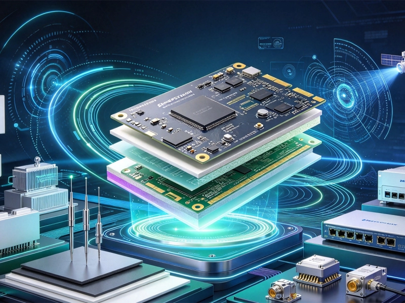
Emerging Trends in High Frequency PCB Materials for Next-Gen CommunicationOctober/10/2026
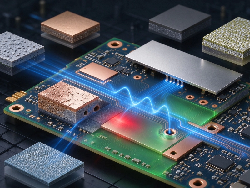
How to Choose the Right High Frequency PCB Material for RF DesignsOctober/21/2026
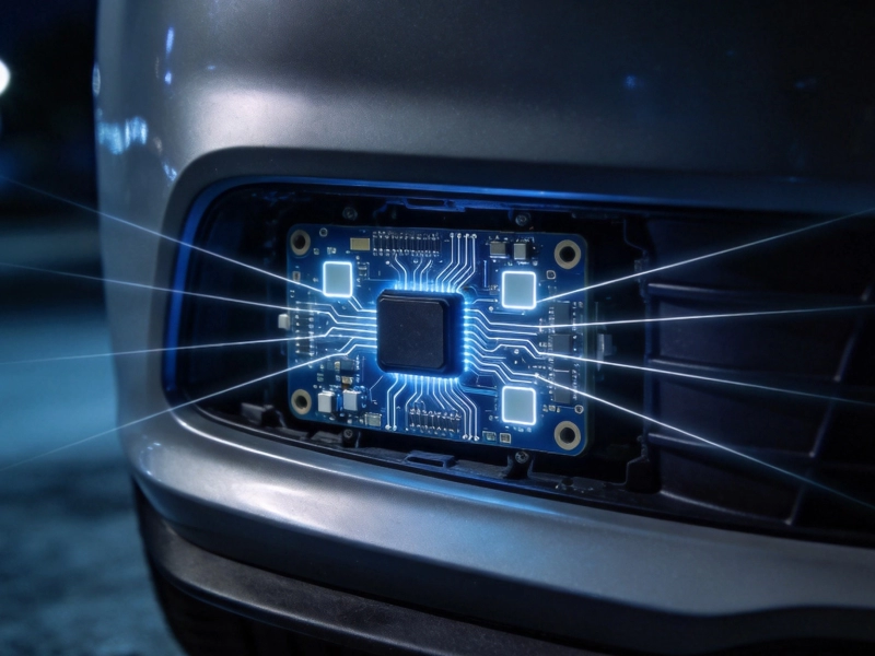
High Frequency PCB Materials for Automotive Radar: Durability and SpeedSeptember/26/2026
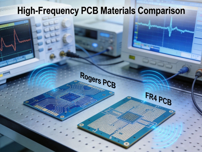
Rogers vs. FR4: Choosing the Right High Frequency PCB MaterialsJune/12/2026