Open Nav

High frequency printed circuit boards (PCBs) have long been associated with Telecommunications Infrastructure, radar systems, and Satellite Communications. But as we look beyond 2026, the application landscape is expanding dramatically. Driven by 6g Research, AI compute scaling, Autonomous Driving, and entirely new paradigms like reconfigurable intelligent surfaces (RIS) and terahertz sensing, high frequency PCBs are entering a period of unprecedented diversification.
This article explores the emerging applications that will shape the high frequency PCB industry from 2027 through 2035, examining the technical requirements, material innovations, and manufacturing challenges each application brings.
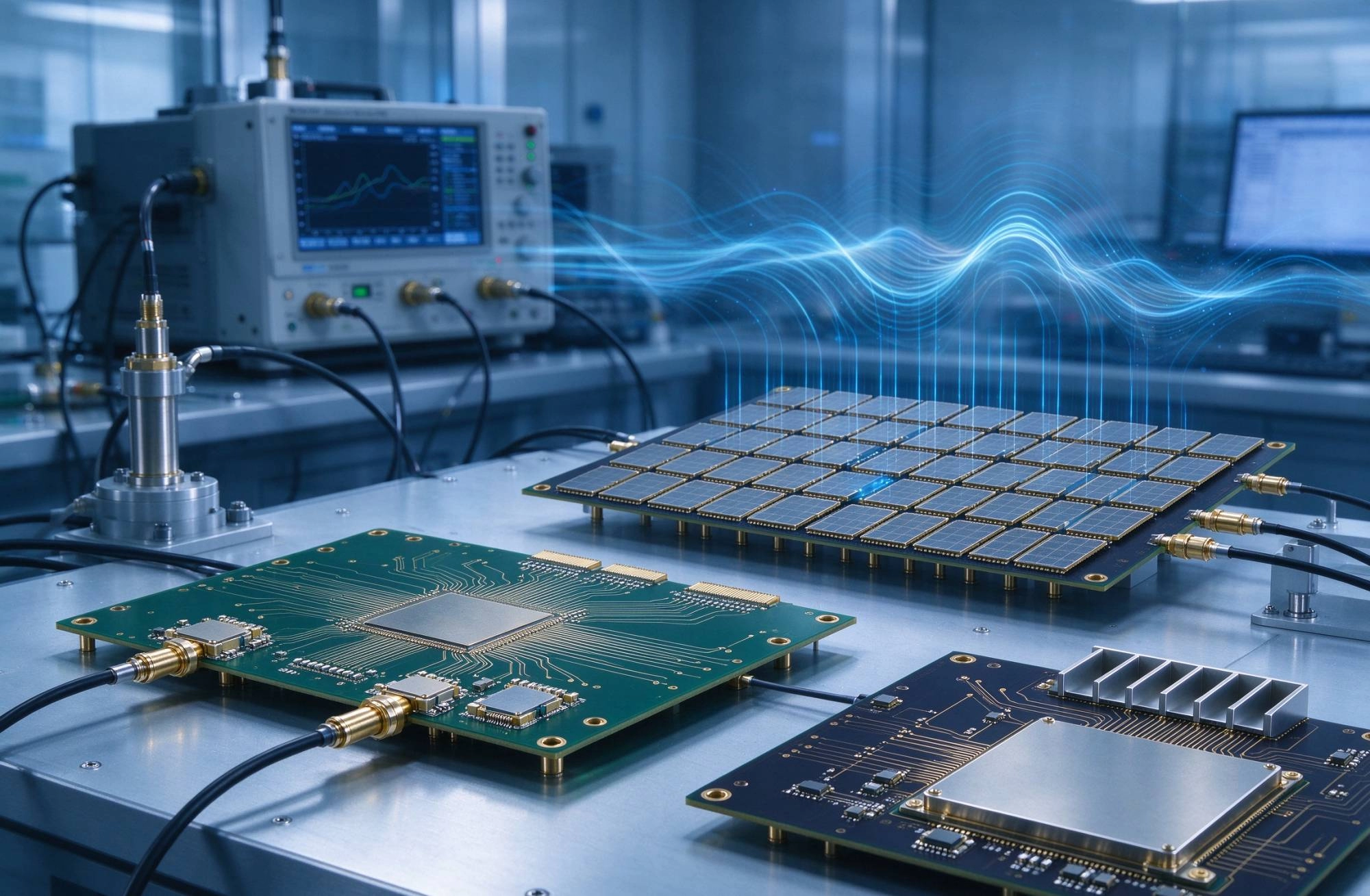
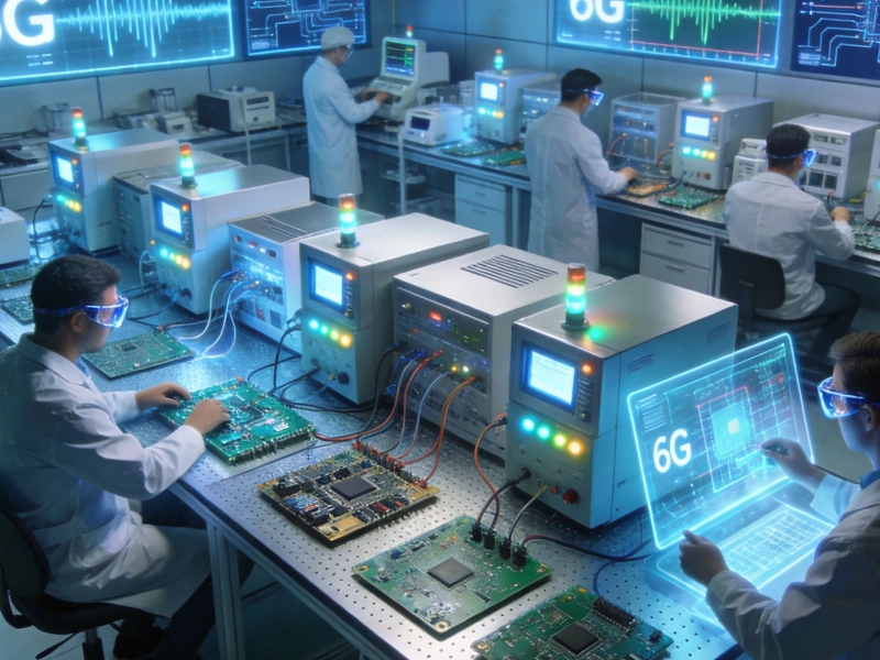
While 5G networks are still being deployed globally, research into 6G is already well underway, with commercial deployment expected around 2030. The defining characteristic of 6G is its use of the terahertz (THz) band — frequencies between 0.1 and 10 THz — which promises data rates 10 to 100 times faster than 5G.
At terahertz frequencies, signal attenuation becomes extreme. Traditional substrate materials like Fr-4 (Df ≈ 0.02) are completely unusable. Even current Low-loss Materials such as Megtron 6 (Df ≈ 0.004) may not suffice. The industry is exploring:
Skin depth at 300 GHz is approximately 0.12 µm in copper. Surface roughness that was acceptable at 28 GHz becomes a dominant loss mechanism at THz frequencies. Ultra-smooth copper foils (Rz ≤ 0.5 µm) and potentially alternative conductors will be required.
AI server platforms are pushing PCB technology at a breathtaking pace. NVIDIA's Rubin GPU platform, expected to reach volume production in late 2026, demands Pcb Materials at the M8/M9 performance tier supporting 224 Gbps and beyond. The next generation — Rubin Ultra — is reportedly targeting 337 Gbps+ signaling rates and will use Ptfe as the primary material for orthogonal backplanes.
This represents a significant shift. PTFE (polytetrafluoroethylene) has long been considered difficult to manufacture due to its poor adhesion and dimensional instability. But its unmatched electrical properties — Dk ≈ 2.1 and Df ≈ 0.001 — make it the only viable option for next-generation AI interconnects. The material ecosystem is expanding rapidly:
AI server PCBs are evolving from traditional multilayer boards into complex hybrid structures:
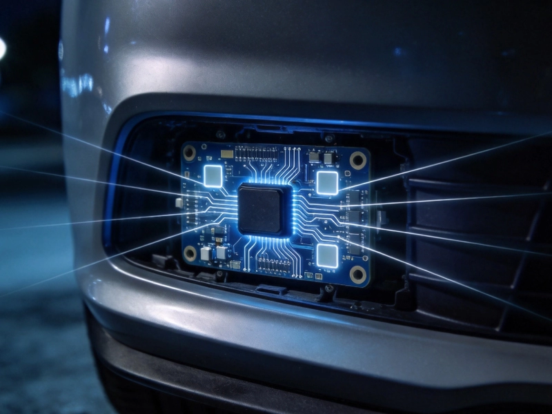
Automotive Radar is transitioning from conventional 77 GHz sensors to 4D imaging radar operating at 79 GHz with significantly wider bandwidth. This enables elevation detection alongside range, azimuth, and velocity — effectively creating a radar "point cloud" comparable to low-resolution LiDAR.
The millimeter-wave Radar Pcb market is projected to grow at approximately 18% CAGR through the early 2030s, driven by Autonomous Driving adoption.
Emerging automotive applications include:
The proliferation of low Earth orbit (LEO) satellite constellations — Starlink, OneWeb, Kuiper, and numerous national systems — is creating sustained demand for space-grade high frequency PCBs.
Satellite PCBs are also trending toward higher integration — combining RF front-end, beamforming ICs, and digital processing on a single board to reduce mass and volume, which directly translates to lower launch costs.
Beyond communications, terahertz frequencies (0.1–10 THz) are opening new sensing and imaging applications:
THz waves can penetrate clothing, paper, and plastic but are reflected by metals and absorbed by water — making them ideal for non-invasive security screening. PCB-based THz sources and detector arrays are being developed for airport and perimeter security systems.
THz imaging can detect subsurface defects in composites, measure coating thickness, and identify contaminants in pharmaceuticals — all without contact or ionizing radiation. High frequency PCBs serve as the platform for THz transmitter and receiver arrays.
Research is exploring THz imaging for early skin cancer detection and dental diagnostics, where THz waves can differentiate between healthy and diseased tissue based on water content differences.
THz circuits demand:
RIS is one of the most conceptually novel applications on the horizon. An RIS is a planar surface composed of hundreds or thousands of individually controllable meta-atoms (unit cells) that can dynamically manipulate electromagnetic waves — reflecting, refracting, or absorbing them on command.
Each meta-atom in an RIS is essentially a small PCB patch with a tunable element (PIN diode, varactor, or MEMS switch). A single RIS panel might contain 1,024 to 4,096 such elements, each requiring:
This creates a unique PCB challenge: large-area panels (potentially 1m × 1m or larger) with extremely high element density, requiring cost-effective manufacturing at scales more typical of display panels than traditional PCBs.
RIS could transform wireless network deployment by turning walls, ceilings, and building facades into programmable signal reflectors — effectively creating "smart radio environments." This would be particularly valuable for 6G indoor coverage and mmWave/THz links that suffer from poor penetration.
As electrical interconnects approach fundamental limits at high frequencies, the industry is exploring hybrid photonic-electronic PCBs that integrate optical waveguides directly into the substrate.
Silicon photonics is already being deployed in data centers through co-packaged optics (CPO), where optical engines are mounted on the same substrate as switch ASICs. The next step is embedding optical waveguides within the PCB itself:
Board-level optical interconnects are expected to move from research prototypes to commercial deployment in the 2028–2032 timeframe, initially in high-end computing and AI systems where electrical loss budgets are exhausted.
The applications described above are only possible because of parallel advances in substrate materials. Key trends include:
| Material System | Dk Range | Df @ 10 GHz | Emerging Application |
|---|---|---|---|
| PTFE (pure) | 2.0–2.2 | 0.0009–0.002 | 224G+ backplanes, THz circuits |
| Ceramic-filled PTFE | 2.5–10.8 | 0.001–0.004 | Automotive Radar, satellite |
| Carbon hydrocarbon resin | 3.0–3.5 | ≤0.0005 (ultra-low) | M9-class AI server PCBs |
| PPO/PPE | 2.8–3.2 | 0.002–0.004 | 5G/6G infrastructure, 112G+ |
| BCB | ~2.3 | <0.0015 | Advanced packaging, mmWave |
| Glass/quartz | 3.7–3.8 | ~0.001 | mmWave/THz interposers |
| Fluorinated PI | 2.8–3.2 | 0.002–0.005 | 6G flexible devices |
| LCP | 2.9–3.1 | 0.002–0.004 | mmWave antennas, flexible RF |
The transition to these emerging applications brings significant manufacturing hurdles:
| Application | Frequency Range | Key PCB Technology | Expected Timeline |
|---|---|---|---|
| AI server 224G+ | Up to 56 GHz (Nyquist) | PTFE backplanes, M8/M9 materials | 2026–2028 |
| 4D imaging radar | 77–81 GHz | Rigid-flex, PTFE laminates | 2025–2030 |
| LEO satellite phased arrays | Ku/Ka/V-band | Large-format, space-grade PTFE | 2025–2035 |
| 6G sub-THz | 100–300 GHz | Glass interposers, fluorinated PI | 2028–2032 |
| THz sensing/imaging | 0.1–10 THz | SIW structures, ultra-smooth Cu | 2028–2035 |
| RIS | Sub-6 to mmWave | Large-area meta-atom arrays | 2028–2035 |
| Photonic PCBs | Optical + RF | Embedded waveguides, CPO | 2028–2032 |
The high frequency PCB industry is transitioning from a supporting role to a central enabling technology. As frequencies climb from GHz to THz, and as applications expand from telecommunications into AI compute, automotive sensing, space infrastructure, and entirely new domains like RIS, PCB manufacturers must invest in new materials, new processes, and new testing capabilities. The companies that succeed will be those that treat high frequency not as a niche specialty but as the foundation of their technology roadmap.
High Frequency PCB Applications for Military Radar and Electronic WarfareSeptember/18/2026
Demystifying Impedance Control: Core High Frequency PCB KnowledgeJuly/09/2026
Top 5 Questions to Ask Your High Frequency PCB Manufacturer Before Placing an OrderAugust/14/2026
Handling Sensitive ComponentsMay/29/2026
Our Latest High Frequency PCB Capabilities for 6G ResearchMay/29/2026

Exploring High Frequency PCB Applications in High-Speed Data CentersSeptember/30/2026
7 Key Factors to Consider When Choosing a High Frequency PCB ManufacturerMay/29/2026
High Frequency PCB Materials for Automotive Radar: Durability and SpeedSeptember/26/2026