Open Nav

high frequency PCB design is equal parts art and science. For RF engineers, translating a simulation that works perfectly in software into a physical board that meets performance targets in the real world often feels like navigating a minefield of unexpected losses, impedance mismatches, and interference issues that never appeared in the model. The difference between a design that works on the first prototype and one that requires three rounds of debug and revision often comes down to following practical, field-proven design guidelines that account for the real-world behavior of materials, manufacturing processes, and high-frequency signals. These guidelines are not arbitrary rules; they are lessons learned from years of debugging failed designs, measuring unexpected losses, and figuring out what works consistently across different materials, frequencies, and manufacturing partners.
This collection of practical guidelines focuses on the design decisions that have the biggest impact on real-world RF performance, from pre-design material selection through prototype validation. Unlike theoretical design textbooks that focus on idealized scenarios, these guidelines are tailored to the trade-offs RF engineers face every day: balancing performance with cost, meeting regulatory requirements, and ensuring designs are manufacturable at volume without sacrificing performance. Whether you are designing a 2.4 GHz IoT radio, a 28 GHz 5G front end, or a 77 GHz Automotive Radar module, these principles will help you avoid the most common pitfalls and get to production faster.
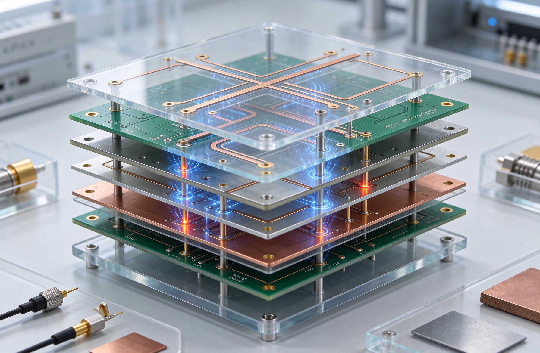
The first and most impactful decision you make in any high frequency design is selecting the right substrate material. Choose incorrectly and you will fight Signal Loss, impedance variation, and thermal issues for the entire design cycle. The good news is you do not always need the most expensive exotic material; the right choice depends on your operating frequency, loss budget, thermal requirements, and cost targets.
Start by defining your requirements clearly before looking at material datasheets. What is your operating frequency range? What is your maximum acceptable Insertion Loss per unit length? What is the expected operating temperature range? Do you have any regulatory requirements for flame resistance or environmental stability? Answering these questions first eliminates 90% of unsuitable materials immediately. For example, if you are designing a low-cost 2.4 GHz Bluetooth module with short transmission paths, high-performance FR4 with Df around 0.008 at 1 GHz is almost certainly sufficient, and spending extra for Rogers or Ptfe material would be a waste of money. If you are designing a 77 GHz Automotive Radar module with long signal paths, you will need a low-loss Ptfe-based material to meet your loss budget. The Skin Effect cause current to concentrate near the conductor surface at high frequencies, so you may also want to specify low-profile copper foil for frequencies above 10 GHz to reduce conductor loss from surface roughness.
Pay close attention to material properties beyond nominal Dk and Df. The thermal coefficient of Dk (TCDk) tells you how much the Dielectric Constant changes with temperature, which is critical for phase-sensitive applications like phased arrays or narrowband filters. A material with TCDk of 50 ppm/°C will experience a 0.01 change in Dk over a 200°C temperature range, which may be enough to shift your filter response out of specification. Moisture absorption is another often-overlooked property; materials that absorb significant moisture will show increased Dk and Df in humid environments, degrading performance over time. For outdoor or industrial applications, select materials with moisture absorption below 0.1% to minimize this effect.
Always confirm material availability with your manufacturer before finalizing your selection. Some specialty materials have long lead times or require minimum order quantities that may not be feasible for your production volume. Your manufacturing partner may also have preferred materials that they process regularly, which can reduce cost and improve yield compared to specifying a rare material they have no experience working with.
The stack-up defines every electrical characteristic of your board, from impedance to signal isolation to thermal performance. A poorly designed stack-up will cause performance issues that no amount of routing optimization can fix. Follow these rules to build a stack-up that meets your performance requirements while remaining manufacturable.
Start with your impedance requirements first. For each Controlled Impedance line in your design (most often 50 ohms for single-ended RF lines and 80 or 100 ohms for differential pairs), calculate the required trace width for your target stack-up using a field solver, not just online calculators that make simplifying assumptions. Make sure the trace width is manufacturable with your selected manufacturer's design rules; a 3 mil trace may give you the exact impedance you want, but if your manufacturer's minimum line width is 4 mils, you will need to adjust the stack-up thickness to allow a wider trace.
Provide continuous, unbroken reference planes for all high-frequency signals. Never route an RF trace over a split in the reference plane; the discontinuity in the return path will cause reflections, increased radiation, and impedance mismatches that degrade performance. If you must cross a split for some reason, add stitching capacitors across the split near the trace to provide a low-impedance return path for high-frequency signals. For designs that mix RF, digital, and power circuits, use separate ground planes for each section connected at a single point to avoid ground loops that can couple noise from digital circuits into sensitive RF sections.
Keep high-frequency signal layers as close to their reference planes as possible for better signal isolation and reduced radiation. Thinner dielectric between the signal layer and reference plane reduces the height of the electromagnetic field above the trace, making it less susceptible to interference from adjacent traces and reducing unintended radiation. A common rule of thumb is to keep the dielectric thickness less than or equal to the trace width for Microstrip lines to minimize field leakage.
Include sufficient copper thickness for power and ground planes to handle current requirements and improve heat spreading. For high-power RF designs, use 2 oz or heavier copper on power and ground planes to reduce resistive loss and improve thermal conductivity. Make sure the stack-up is symmetric to avoid board warping during lamination; a symmetric stack-up with equal numbers of copper layers on both sides of the center core will have less residual stress and be less likely to warp during assembly or temperature cycling.
High frequency signals travel along Transmission Lines, not simple traces. Small mistakes in Transmission Line design can cause significant Signal Loss, reflection, and interference that can kill your link budget before the signal even leaves the board. Follow these guidelines to design Transmission Lines that perform as expected.
Choose the right Transmission Line type for your application. Microstrip lines (trace on outer layer, reference plane directly below) are the most common and easiest to manufacture, but they radiate more and are more susceptible to interference from adjacent layers. Grounded Coplanar Waveguide (Gcpw), which adds ground planes on the same layer as the signal trace adjacent to the line, provides better isolation and more consistent impedance, making it ideal for frequencies above 10 GHz or for designs where noise isolation is critical. Stripline (trace between two reference planes) provides the best isolation and lowest radiation, but it requires more layers and makes testing more difficult because the traces are buried inside the board.
Avoid right-angle bends in RF transmission lines. The sharp corner creates a discontinuity in the line width and an impedance mismatch that causes reflections and radiation. Use 45-degree bends or curved bends with radius at least three times the trace width instead. For differential pairs, keep the pair length matched within the tolerance required by your protocol, and make sure the distance between the pair (the coupling) remains constant along the entire length to avoid impedance variation.
Minimize via usage in high-frequency signal paths wherever possible. Vias introduce impedance discontinuities, stubs, and additional loss that degrade performance. If you must use a via to transition between layers, design it as an impedance-controlled via with surrounding ground stitching vias to provide a continuous return path. For frequencies above 6 GHz, back-drill vias to remove the unused stub portion that causes resonance and signal reflections. Always simulate the via structure with a 3D electromagnetic solver to characterize its impedance and Insertion Loss before including it in a critical signal path.
Provide adequate clearance around RF traces to avoid coupling to adjacent traces. The clearance required depends on the signal frequency and the trace height above the reference plane; a good starting point is to keep adjacent traces at least three times the trace width apart to minimize crosstalk. For sensitive RF inputs or high-power outputs, increase clearance to five times the trace width or add grounded guard traces between signal lines for additional isolation.
How you place components and route traces has as much impact on performance as your stack-up and material selection. Poor placement can introduce noise, loss, and interference that you cannot eliminate after the fact.
Keep high-frequency signal paths as short as possible. Every millimeter of extra trace adds insertion loss and increases the risk of interference. Place RF components in a logical signal flow order, starting from the antenna input, through the filter, low-noise amplifier, mixer, and so on, with minimal backtracking or crossing of signal paths. Group related components together to minimize trace length between them; for example, place the matching network components as close to the amplifier input and output pins as possible to minimize stub length and loss.
Isolate sensitive Rf Circuits from noisy digital and power circuits. Place high-power RF output sections as far as possible from low-noise receiver inputs to avoid desensitizing the receiver from transmitted signal leakage. If the board includes both high-speed digital circuits and Rf Circuits, place them on opposite sides of the board or separate them with grounded metal fences to block Electromagnetic Interference. Use separate power supplies for RF and digital sections, with ferrite beads or LC filters on the supply lines to prevent digital noise from coupling into the RF power rail.
Place decoupling capacitors as close to IC power pins as possible, with multiple capacitor values to filter noise across the entire frequency range. A 0.1 µF ceramic capacitor placed within 1 mm of the power pin handles high-frequency noise, while a larger 1 µF or 10 µF capacitor placed nearby filters lower frequency ripple. For high-power RF amplifiers, use multiple parallel decoupling capacitors on the supply line to provide low impedance across the full operating bandwidth and prevent supply line oscillations.
Ground all unused board area with copper pour connected to the Ground Plane Via Stitching vias spaced at regular intervals (typically 1/10 of the wavelength at your highest operating frequency). Stitching vias reduce radiation from the board, provide a low-impedance ground connection, and prevent the formation of unwanted resonant cavities in empty areas of the board. Avoid leaving large areas of floating copper that can act as antennas and radiate unintended signals.
High frequency circuits, especially power amplifiers and transmitters, generate significant heat that can degrade performance and reduce component lifespan if not dissipated effectively. Thermal Management should be considered from the earliest stages of design, not added as an afterthought.
Place high-power components near the edge of the board or near a connection to an external heatsink where possible. Use thermal vias under high-power components to conduct heat from the component package to the Ground Plane or an external heatsink. For components with exposed thermal pads, use a solid copper pad directly under the component connected to multiple thermal vias to maximize heat transfer; avoid using solder mask over the thermal pad unless the component datasheet specifically requires it.
Use thick copper planes for ground and power layers to spread heat across the board more effectively. A 2 oz copper plane conducts heat almost twice as well as a 1 oz plane, reducing hot spot temperatures significantly. For very high-power designs, consider using a metal core PCB or an insulated metal substrate (IMS) to provide a direct thermal path to an external heatsink.
Account for thermal effects on performance during design. Changes in temperature affect component parameters, Dielectric Constant, and line impedance, which can shift the operating frequency of filters and oscillators or reduce amplifier efficiency. Simulate your design performance across the full expected operating temperature range to ensure it remains within specification even at temperature extremes.
A design that works perfectly in simulation but cannot be manufactured consistently at volume is useless for real-world products. Follow these Dfm guidelines to ensure your design can be produced reliably with high yield.
Always adhere to your manufacturer's published design rules for minimum line width, minimum spacing, minimum via size, and minimum annular ring. If you push the limits of their capabilities, you will see lower yield and higher cost. If your design requires features smaller than their standard capabilities, discuss it with them first to confirm they can achieve it consistently and understand any additional cost or yield impact.
Include test points for all critical RF signals, power rails, and ground connections to simplify testing and debug. Use exposed pads on the outer layer for test points, with sufficient clearance around them for probe access. For high-frequency measurements, include calibrated test structures like TRL (Thru-Reflect-Line) or SOLT (Short-Open-Load-Thru) calibration standards on the panel to enable accurate de-embedding of probe and fixture losses during characterization.
Provide clear, unambiguous documentation to your manufacturer. Include a detailed stack-up drawing with material specifications, dielectric thicknesses, copper weights, and impedance requirements. Provide clear notes on any special requirements, such as via back-drilling, controlled depth routing, or special surface finishes. Do not assume the manufacturer will know what you want; explicit documentation eliminates ambiguity.
Request a design for manufacturability (Dfm) review from your manufacturer before starting production. They will identify issues like insufficient annular ring, acid traps, or features that are too small to manufacture reliably. Making small adjustments to the design based on their feedback will almost always improve yield and reduce cost without affecting performance.
Even the most carefully designed board will have unexpected performance issues that do not show up in simulation. Prototyping and validation are critical steps to catch these issues before you commit to Mass Production.
Build a small prototype run first, even for simple designs. Test critical parameters including impedance, insertion loss, return loss, and output power to confirm they match simulation results. If performance does not match expectations, use a combination of simulation and measurement to identify the root cause. Common discrepancies include unaccounted for via losses, higher than expected material loss, or unexpected coupling between traces.
Use de-embedding techniques to remove the effect of test fixtures and probes from your measurements. The loss and impedance mismatch of the test setup can easily obscure the actual performance of your circuit, especially at high frequencies. Use on-board calibration standards to characterize the test setup and remove its effect from your measurements for more accurate results.
Test your design across the full range of operating conditions, including temperature extremes, supply voltage variations, and expected load conditions. A design that works perfectly at room temperature may fail at high temperature when component parameters drift and dielectric properties change. Environmental testing will catch these issues before they cause field failures.
Even experienced RF engineers make predictable mistakes that degrade performance. Watch for these common pitfalls:
Forgetting about via stubs: An unbackdrilled via stub can cause significant resonance and loss at frequencies where the stub length is a quarter wavelength. Always backdrill vias for designs operating above 6 GHz, or use blind vias to avoid stubs entirely.
Ignoring return path discontinuities: A signal trace crossing a split in the ground plane is one of the most common causes of Emi issues and Signal Integrity problems. Always ensure high-frequency signals have a continuous return path directly below the trace.
Over-specifying materials: You do not need the most expensive low-loss PTFE material for a 2.4 GHz design with short trace lengths. Using a lower-cost high-performance FR4 material will meet your requirements and reduce cost significantly.
Neglecting decoupling: Poor power supply decoupling causes noise that can degrade receiver sensitivity or cause amplifier instability. Use multiple Decoupling Capacitor values placed as close to the IC pins as possible to provide low impedance across the full operating bandwidth.
high frequency PCB design is a discipline that rewards attention to detail and practical experience as much as theoretical knowledge. Following these guidelines will help you avoid the most common pitfalls, reduce prototype iterations, and get to production faster with designs that perform as expected. The key is to balance theoretical performance requirements with practical manufacturing constraints, and to work closely with your manufacturing partner early in the design process to ensure your design is both high-performance and manufacturable at scale.
As high frequency applications continue to expand into 5G, automotive radar, Satellite Communications, and IoT markets, these design principles will only become more important. Building expertise in practical high frequency design is a valuable skill that will remain in high demand for years to come.
Contact us to discuss your requirements and explore how our high frequency pcb design and manufacturing capabilities can support your RF projects.
Key High Frequency PCB Knowledge for Successful RF Circuit DesignSeptember/07/2026

Essential High Frequency PCB Knowledge for Hardware Engineers and DesignersJune/15/2026
High Frequency PCB Knowledge: Best Practices for Grounding and ShieldingOctober/12/2026

High Frequency PCB Knowledge: Managing Crosstalk and EMI in Dense LayoutsAugust/11/2026

Demystifying Impedance Control: Core High Frequency PCB KnowledgeJuly/09/2026

High Frequency PCB Knowledge: The Difference Between High-Speed and High-FrequencySeptember/17/2026
The Engineer's Guide to High Frequency PCB Knowledge and Stack-up DesignJuly/31/2026
High Frequency PCB vs High Speed PCB: When to Use EachNovember/02/2026